- 您现在的位置:买卖IC网 > PDF目录369515 > BT16899DL (NXP SEMICONDUCTORS) 18-bit latched transceiver with 16-bit parity generator/checker 3-State PDF资料下载
参数资料
| 型号: | BT16899DL |
| 厂商: | NXP SEMICONDUCTORS |
| 元件分类: | 通用总线功能 |
| 英文描述: | 18-bit latched transceiver with 16-bit parity generator/checker 3-State |
| 中文描述: | ABT SERIES, DUAL 8-BIT REGISTERED TRANSCEIVER, TRUE OUTPUT, PDSO56 |
| 封装: | 7.50 MM, PLASTIC, MO-118AB, SOT-371-1, SSOP-56 |
| 文件页数: | 7/16页 |
| 文件大小: | 105K |
| 代理商: | BT16899DL |
Philips Semiconductors
Product specification
74ABT16899
74ABTH16899
18-bit latched transceiver with 16-bit
parity generator/checker (3-State)
1998 Feb 25
7
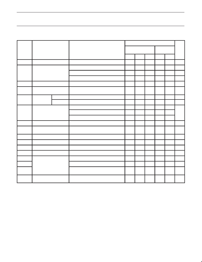
DC ELECTRICAL CHARACTERISTICS
LIMITS
SYMBOL
PARAMETER
TEST CONDITIONS
T
amb
= +25
°
C
T
amb
= –40
°
C
to +85
°
C
UNIT
Min
Typ
Max
Min
Max
V
IK
Input clamp voltage
V
CC
= 4.5V; I
IK
= –18mA
–0.7
–1.2
–1.2
V
V
CC
= 4.5V; I
OH
= –3mA; V
I
= V
IL
or V
IH
2.5
3.1
2.5
V
V
OH
High-level output voltage
V
CC
= 5.0V; I
OH
= –3mA; V
I
= V
IL
or V
IH
3.0
3.6
3.0
V
V
CC
= 4.5V; I
OH
= –32mA; V
I
= V
IL
or V
IH
2.0
2.7
2.0
V
V
OL
Low-level output voltage
V
CC
= 4.5V; I
OL
= 64mA; V
I
= V
IL
or V
IH
0.36
0.55
0.55
V
V
RST
Power-up output low
voltage
3
V
CC
= 5.5V; I
O
= 1mA; V
I
= GND or V
CC
0.13
0.55
0.55
V
I
I
Input leakage
Control pins
V
CC
= 5.5V; V
I
= GND or 5.5V
V
CC
= 5.5V; V
I
= GND or 5.5V
±
0.2
±
1.0
±
1.0
μ
A
current
Data pins
±
1.0
±
100
±
100
μ
A
Bushold current A or B
inputs
5
74ABTH16899
V
CC
= 4.5V; V
I
= 0.8V
V
CC
= 4.5V; V
I
= 2.0V
75
75
I
HOLD
–75
–75
μ
A
V
CC
= 5.5V; V
I
= 0 to 5.5V
±
500
I
OFF
Power-off leakage current
V
CC
= 0.0V; V
O
or V
I
≤
4.5V
±
2.0
±
100
±
100
μ
A
I
PU
/I
PD
Power-up/down 3-State
output current
4
V
CC
= 2.1V; V
O
= 0.5V; V
I
= GND or V
CC
±
5.0
±
50
±
50
μ
A
I
IH
+ I
OZH
3-State output High current
V
CC
= 5.5V; V
O
= 2.7V; V
I
= V
IL
or V
IH
2.0
50
50
μ
A
I
IL
+ I
OZL
3-State output Low current
V
CC
= 5.5V; V
O
= 0.5V; V
I
= V
IL
or V
IH
–2.0
–50
–50
μ
A
I
CEX
Output High leakage current
V
CC
= 5.5V; V
O
= 5.5V; V
I
= GND or V
CC
2.0
50
50
μ
A
I
O
Output current
1
V
CC
= 5.5V; V
O
= 2.5V
–50
–100
–180
–50
–180
mA
I
CCH
V
CC
= 5.5V; Outputs High, V
I
= GND or V
CC
0.5
1
1
mA
I
CCL
Quiescent supply current
V
CC
= 5.5V; Outputs Low, V
I
= GND or V
CC
10.5
19
19
mA
I
CCZ
V
CC
= 5.5V; Outputs 3-State;
V
I
CC
0.5
1
1
mA
I
CC
Additional supply current per
input pin
2
V
CC
= 5.5V; one input at 3.4V,
other inputs at V
CC
or GND
0.2
1.5
1.5
mA
NOTES:
1. Not more than one output should be tested at a time, and the duration of the test should not exceed one second.
2. This is the increase in supply current for each input at 3.4V.
3. For valid test results, data must not be loaded into the flip-flops (or latches) after applying the power.
4. This parameter is valid for any V
CC
between 0V and 2.1V, with a transition time of up to 10msec. From V
CC
= 2.1V to V
CC
= 5V
±
10%, a
transition time of up to 100
μ
sec is permitted.
5. This is the bus hold overdrive current required to force the input to the opposite logic state.
相关PDF资料 |
PDF描述 |
|---|---|
| BT168BW | Thyristors logic level for RCD/ GFI/ LCCB applications(应用于RCD/ GFI/ LCCB的可控硅逻辑电平) |
| BT168EW | Thyristors logic level for RCD/ GFI/ LCCB applications |
| BT168W | Thyristors logic level for RCD/ GFI/ LCCB applications |
| BT168WSERIES | Thyristors logic level for RCD/ GFI/ LCCB applications |
| BT168DW | Thyristors logic level for RCD/ GFI/ LCCB applications(应用于RCD/ GFI/ LCCB的可控硅逻辑电平) |
相关代理商/技术参数 |
参数描述 |
|---|---|
| BT168B | 制造商:PHILIPS 制造商全称:NXP Semiconductors 功能描述:Thyristors logic level for RCD/ GFI/ LCCB applications |
| BT168BW | 制造商:PHILIPS 制造商全称:NXP Semiconductors 功能描述:Thyristors logic level for RCD/ GFI/ LCCB applications |
| BT168D | 制造商:PHILIPS 制造商全称:NXP Semiconductors 功能描述:Thyristors logic level for RCD/ GFI/ LCCB applications |
| BT168DW | 制造商:PHILIPS 制造商全称:NXP Semiconductors 功能描述:Thyristors logic level for RCD/ GFI/ LCCB applications |
| BT168E | 功能描述:SCR BULK MOSFET RoHS:否 制造商:STMicroelectronics 最大转折电流 IBO:480 A 额定重复关闭状态电压 VDRM:600 V 关闭状态漏泄电流(在 VDRM IDRM 下):5 uA 开启状态 RMS 电流 (It RMS): 正向电压下降:1.6 V 栅触发电压 (Vgt):1.3 V 最大栅极峰值反向电压:5 V 栅触发电流 (Igt):35 mA 保持电流(Ih 最大值):75 mA 安装风格:Through Hole 封装 / 箱体:TO-220 封装:Tube |
发布紧急采购,3分钟左右您将得到回复。