- 您现在的位置:买卖IC网 > PDF目录256172 > BU-61688F0-100Z (DATA DEVICE CORP) 2 CHANNEL(S), 1M bps, MIL-STD-1553 CONTROLLER, CQFP72 PDF资料下载
参数资料
| 型号: | BU-61688F0-100Z |
| 厂商: | DATA DEVICE CORP |
| 元件分类: | 微控制器/微处理器 |
| 英文描述: | 2 CHANNEL(S), 1M bps, MIL-STD-1553 CONTROLLER, CQFP72 |
| 封装: | 1 X 1 INCH, LOW PROFILE, CERAMIC, QFP-72 |
| 文件页数: | 6/12页 |
| 文件大小: | 141K |
| 代理商: | BU-61688F0-100Z |
3
Data Device Corporation
www.ddc-web.com
BU-65178/65179*/61688*/61689*
F1 web-09/02-0
CLOCK INPUT
! Long Term Tolerance
1553A Mode
1553B Mode
! Short Term Tolerance, 1 second
1553A Mode
1553B Mode
! Duty Cycle
16 MHz
12 MHz
10 MHz*
20 MHz
oz
(g)
in.
(mm)
in.
(mm)
0.6
(17)
1.0 X 1.0 X 0.150
(25.4 x 25.4 x 3.81)
1.0 X 1.0 X 0.155
(25.4 x 25.4 x 3.94)
PHYSICAL CHARACTERISTICS
Size
! BU-65178/61588 P
BU-65179*/61688*/61689*
! BU-65178/61588 F/G
BU-65179*/61688*/61689*
Weight
! BU-65178/61588 F/P/G
BU-65179*/61688*/61689*
°C/W
°C
0.01
0.1
0.001
0.01
67
60
6.8
150
+300
16.0
12.0
-55
-65
THERMAL
Thermal Resistance, Junction-to-Case,
Hottest Die (
θJC)
! BU-65178/61588X3*
Operating Junction Temperature
Storage Temperature
Lead Temperature (soldering, 10 sec.)
UNITS
MAX
TYP
MIN
PARAMETER
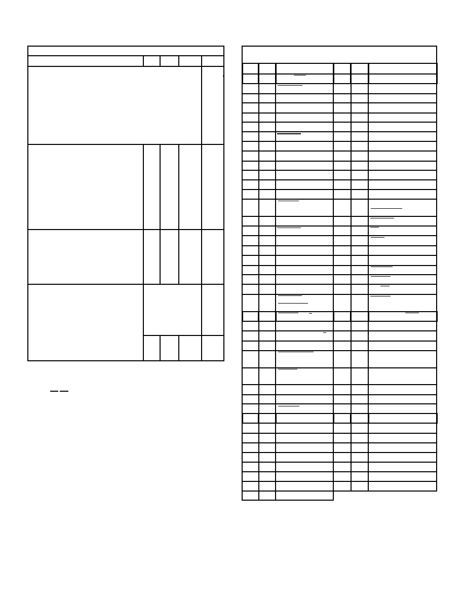
TABLE 1. BU-65178/65179*/61588/61688*/61689*SPECIFICATIONS (cont’d)
Notes: Notes 1 through 6 are applicable to the Receiver Differential
Resistance and Differential Capacitance specifications:
(1) Specifications include both transmitter and receiver (tied together internally).
(2) Measurement of impedance is directly between pins TX/RX A(B)
and TX/RX A(B) of the BU-65178/61588X3 hybrid.
(3) Assuming the connection of all power and ground inputs to the hybrid.
(4) The specifications are applicable for both unpowered and powered conditions.
(5) The specifications assume a 2 volt rms balanced, differential, sinu-
soidal input. The applicable frequency range is 75 kHz to 1 MHz.
(6) Minimum resistance and maximum capacitance parameters are
guaranteed, but not tested, over the operating range.
(7) Assumes a common mode voltage within the frequency range of dc to 2
MHz, applied to pins of the isolation transformer on the stub side (either direct
or transformer coupled), referenced to hybrid ground. Use a DDC recom-
mended transformer or other transformer that provides an equivalent CMRR.
(8) Typical value for minimum intermessage gap time. Under software
control, may be lengthened to (65,535
s minus message time), in
increments of 1
s.
(9) Software programmable (4 options). Includes RT-to-RT Timeout (Mid-
Parity of Transmit Command to Mid-Sync of Transmitting RT Status).
(10) For both +5 V logic and transceiver. +5 V for channels A and B.
(11) Measured from mid-parity crossing of Command Word to mid-sync
crossing of RT’s Status Word.
(12) External 10
F Tantalum and 0.1 F capacitors should be located
as close as possible to Pins 20 and 72 on the Flat Package
and Pins A9 and J3 on the PGA package, and 0.1
F at Pin 37/D3.
(13) MIL-STD–1760 requires that the Mini-ACE produce a 20 Vp-p min-
imum output on the stub connection.
33
40
Frequency
! BU-61588/61688*/65178
Default Mode
16
MHz
Software Programmable Option
12
MHz
! BU-61689*
Default Mode
20
MHz
Software Programmable Option
10
MHz
! BU-65179*
Pin Programmable Option
10/12/16/20
MHz
%
TABLE 2. BU-65178 / 65179* /61588 /61688*/61689* PIN LISTINGS
(QFP-QUAD FLAT PACK, PGA-PIN GRID ARRAY AND GULL LEAD)
35
RTAD4
**
QFP
NAME
QFP
NAME
1
MEM/REG
42
D00
2
MSTCLR
43
D02
3
A11
44
D03
4
A10
45
D05
5
TX/RX-A
46
D08
6
A08
47
7
D07
TX/RX-A
48
8
D13
A14, See NOTE 1
49
D12
9
A04
50
D14
10
A03
51
D09
11
A07
52
D11
12
A02
53
D15
13
TX/RX-B
54
D10
14
MEMOE/ADDR_LAT
55
TRANSPARENT/
BUFFERED
15
A00
56
READYD
16
TX/RX-B
57
INT
17
LOGIC GND
58
IOEN
18
LOGIC GND
59
TX_INH_A
19
LOGIC GND
60
TX_INH_B
20
+5V VCC2
61
SELECT
21
RTAD2
62
STRBD
22
A06
63
RD/WR
23
MEMWR/
ZEROWAIT
64
DTGRT/MSB/LSB
24
DTREQ/16/8
65
Test Output (RX-A)
25
Test Output (RX-B)
66
A15, See NOTE 1
26
Test Output (RX-B)
67
Test Output (RX-A)
27
A01
68
A05
28
MEMENA_IN/
TRIGGER_SEL
69
A09
29
DTACK/
POLARITY_SEL
70
A12, See NOTE 2
30
CLOCK_IN
71
A13, See NOTE 3
31
RT_AD_LAT
72
+5V VCC1
32
SSFLAG/EXT_TRIG
**
Test Output (A_RExt)
33
RTAD0
**
Test Output (A_Test1)
34
RTAD3
**
Test Output (AB_Test4)
Test Output (B_RExt)
36
D06
**
Test Output (AB_Tstck)
H8
PGA
B4
B5
C2
C3
C1
D2
D1
C4
E3
F2
E1
F3
G1
G4
G3
H1
A7
A8
J8
A9
J7
F1
J2
H5
H3
H4
G2
J5
J6
H6
G7
H2
H7
G8
E8
E4
PGA
H9
F9
F7
G5
E7
E9
D7
B2
D9
B9
A2
D8
A1
C9
B8
C8
A3
B7
C7
C6
A6
A5
J1
A4
C5
B6
E2
J4
B3
B1
J3
D4
D5
D6
E6
37
D3
+5V VCC
**
F4
Test Output (AB_Test2)
38
F8
D01
**
F5
Test Output (AB_Test3)
39
G6
D04
**
F6
Test Output (B_Test1)
40
G9
RTADP
N/A
E5
No Connect
41
J9
RTAD1
NOTES
** Note that the Test Output pins on the flat pack are pads located on
the bottom of the package.
1. BU-65179*, A15/A14 pins are actually CLK SEL 1 / CLK SEL 0 respectively.
2. BU-65179*, A12 pin selects the RT_BOOT_L OPTIONAL MODE.
3. BU-65179*, A13 pin has no connection.
相关PDF资料 |
PDF描述 |
|---|---|
| BU-61688F0-410 | 2 CHANNEL(S), 1M bps, MIL-STD-1553 CONTROLLER, CQFP72 |
| BU-61688F0-420Z | 2 CHANNEL(S), 1M bps, MIL-STD-1553 CONTROLLER, CQFP72 |
| BU-61688F0-460L | 2 CHANNEL(S), 1M bps, MIL-STD-1553 CONTROLLER, CQFP72 |
| BU-61688F3-100K | 2 CHANNEL(S), 1M bps, MIL-STD-1553 CONTROLLER, CQFP72 |
| BU-61688F3-102K | 2 CHANNEL(S), 1M bps, MIL-STD-1553 CONTROLLER, CQFP72 |
相关代理商/技术参数 |
参数描述 |
|---|---|
| BU-61688F3 | 制造商:未知厂家 制造商全称:未知厂家 功能描述:MINIATURE ADVANCED COMMUNICATION ENGINE (MINI-ACE) AND MINI-ACE PLUS |
| BU-61688F3-102 | 制造商:未知厂家 制造商全称:未知厂家 功能描述:MIL-STD-1553/ARINC Bus Controller/RTU |
| BU-61688F3-112 | 制造商:未知厂家 制造商全称:未知厂家 功能描述:MIL-STD-1553/ARINC Bus Controller/RTU |
| BU-61688F3-122 | 制造商:未知厂家 制造商全称:未知厂家 功能描述:MIL-STD-1553/ARINC Bus Controller/RTU |
| BU-61688G0 | 制造商:未知厂家 制造商全称:未知厂家 功能描述:MINIATURE ADVANCED COMMUNICATION ENGINE (MINI-ACE) AND MINI-ACE PLUS |
发布紧急采购,3分钟左右您将得到回复。