- 您现在的位置:买卖IC网 > PDF目录166601 > BU-63149D3-220K Transceiver PDF资料下载
参数资料
| 型号: | BU-63149D3-220K |
| 元件分类: | 收发器 |
| 英文描述: | Transceiver |
| 中文描述: | 收发器 |
| 文件页数: | 3/8页 |
| 文件大小: | 65K |
| 代理商: | BU-63149D3-220K |
3
INTRODUCTION
The BU-63147/49 is a dual redundant transmitter and receiver
packaged in a 36-pin DDIP. It is directly compatible to Harris
15530 encoder/decoder and has internal (factory preset) thresh-
old levels. The dual transceiver only requires +5V power and
conforms to MIL-STD-1553A and 1553B. For McAir compatabili-
ty, versions are available with rise/fall times of 200 to 300 nsec.
FIGURE 3 illustrates the connection between a BU-63147/49
transceiver and a MIL-STD-1553 Data Bus. After transformer
isolating the transceiver, it can be either direct coupled (short
stub) or transformer coupled (long stub) to the Data Bus.
TRANSMIT OPERATING MODE
The transmitter section accepts encoded TTL data and converts
it to phase-modulated bipolar form using a waveshaping network
and driver circuits. The driver outputs TX DATA OUT and
are transformer coupled to the Data Bus.
The transmitter output terminals can be put into a high imped-
ance state by setting INHIBIT high, or setting TX DATA IN and
to the same logic level. The operating modes are
shown in TABLE 2.
The transceivers are able to operate in a “wraparound” mode.
This allows output data to be monitored by the receiver section
and returned to the decoder where it is checked for errors.
IN
DATA
TX
OUT
DATA
TX
OFF
X
1
TX DATA OUT ON,
TX DATA OUT OFF
L
0
1
TX DATA OUT ON,
TX DATA OUT OFF
L
1
0
OFF
X
0
OFF (NOTE)
H
X
DRIVER OUTPUT
TX INHIBUIT
TX Data In
TABLE 2. TRANSMIT OPERATING MODE
RECEIVER OPERATING MODE
The receiver section accepts data from a MIL-STD-1553 Data
Bus when coupled to the Data Bus as shown in FIGURE 3. This
data
is
converted
to
bi-phase TTL
and
furnished
to
RX DATA OUT and
.
When STROBE is high data passes throught the receiver to
RX DATA OUT and
. Applying a low to STROBE
disables the receiver output terminals.
As illustrated in FIGURE 2, the receiver in the BU-65147 pro-
vides compatibility to the Harris decoder, while the BU-63149
provides compatibility to the Smiths decoder.
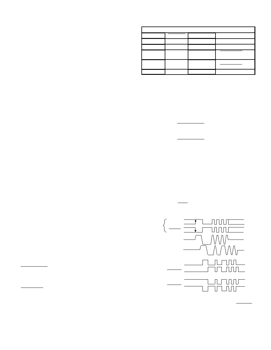
WAVEFORMS
FIGURE 2 illustrates the BU-63147 with Harris type decoder
interface and the BU-63149 with Smiths type decoder interface.
Note that DATA and
inputs must be complementary wave-
forms with a 50% duty cycle.
DATA
OUT
DATA
RX
OUT
DATA
RX
NOTE:
DRIVER OUTPUT terminals are in the high impedance mode
during OFF time, independent of INHIBIT status.
FIGURE 2. WAVEFORMS FOR HARRIS/SMITHS
TYPE ENCODER/DECODERS
X X X
ENCODER
OUTPUT
(NOTE 2)
TX Data In
LINE-TO-LINE
OUTPUT
LINE-TO-LINE
INPUT
RX Data Out
Notes:
(1) TX Data In and RX Data Out are TTL signals.
(2) TX Data In inputs must be at opposite logic levels during transmission, and at
the same logic level when not transmitting.
(3) LINE-TO-LINE output voltage is measured between TX Data Out and TX Data Out.
(4) LINE-TO-LINE input voltage is measured on the Data Bus.
RX Data Out
BU-63147
BU-63149
(4) The specifications are applicable for both unpowered and powered conditions.
(5) The specifications assume a 2 volt rms balanced, differential, sinusoidal input.
The applicable frequency range is 75 kHz to 1 MHz.
(6) Minimum resistance and maximum capacitance parameters are guaranteed
over the operating range, but are not tested.
(7) The Threshold Level, as referred to in this specification, is meant to be the
maximum peak-to-peak voltage (measured on the data bus) that can be
applied to the receiver's input without causing the output to change from the
OFF state.
(8) Assumes a common mode voltage within the frequency range of dc to 2 MHz,
applied to pins of the isolation transformer on the stub side (either direct or
transformer coupled), and referenced to transceiver ground. Transformer must
be a DDC recommended transformer or other transformer that provides an
equivalent minimum CMRR.
(9) MIL-STD-1760 requires minimum output voltage of 20 Vp-p on the stub con-
nection. The -XX2 option is not available for the BU-63147X4 version.
(10) Power dissipation specifications assume a transformer coupled configura-
tion, with external dissipation (while transmitting) of 0.14 watts for the active
isolation transformer, 0.08 watts for the active coupling transformer, 0.45 watts
for each of the two bus isolation resistors, and 0.15 watts for each of the two
bus termination resistors.
Notes (continued)
相关PDF资料 |
PDF描述 |
|---|---|
| BU-63149D3-220S | Transceiver |
| BU-63149D3-220Y | Transceiver |
| BU-63149D3-222K | Transceiver |
| BU-63149D3-222S | Transceiver |
| BU-63149D3-222Y | Transceiver |
相关代理商/技术参数 |
参数描述 |
|---|---|
| BU-63149D3-220S | 制造商:未知厂家 制造商全称:未知厂家 功能描述:Transceiver |
| BU-63149D3-220Y | 制造商:未知厂家 制造商全称:未知厂家 功能描述:Transceiver |
| BU-63149D3-222K | 制造商:未知厂家 制造商全称:未知厂家 功能描述:Transceiver |
| BU-63149D3-222S | 制造商:未知厂家 制造商全称:未知厂家 功能描述:Transceiver |
| BU-63149D3-222Y | 制造商:未知厂家 制造商全称:未知厂家 功能描述:Transceiver |
发布紧急采购,3分钟左右您将得到回复。