- 您现在的位置:买卖IC网 > PDF目录255989 > BU-63825D0-191 (DATA DEVICE CORP) 2 CHANNEL(S), 1M bps, MIL-STD-1553 CONTROLLER, CQIP70 PDF资料下载
参数资料
| 型号: | BU-63825D0-191 |
| 厂商: | DATA DEVICE CORP |
| 元件分类: | 微控制器/微处理器 |
| 英文描述: | 2 CHANNEL(S), 1M bps, MIL-STD-1553 CONTROLLER, CQIP70 |
| 封装: | CERAMIC, DIP-70 |
| 文件页数: | 29/48页 |
| 文件大小: | 405K |
| 代理商: | BU-63825D0-191 |
第1页第2页第3页第4页第5页第6页第7页第8页第9页第10页第11页第12页第13页第14页第15页第16页第17页第18页第19页第20页第21页第22页第23页第24页第25页第26页第27页第28页当前第29页第30页第31页第32页第33页第34页第35页第36页第37页第38页第39页第40页第41页第42页第43页第44页第45页第46页第47页第48页
35
Data Device Corporation
www.ddc-web.com
BU-63825
C-02/06-0
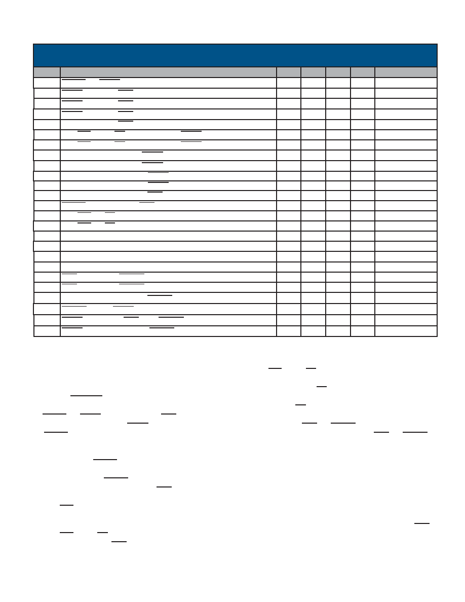
Notes for FIGURE 17 and associated table.
1. For the 16-bit buffered configuration, the inputs TRIGGER_SEL and
MSB/LSB may be connected to +5 V or GND. For the nonzero wait
interface, ZEROWAIT must be connected to logic “1.”
2. SELECT and STRBD may be tied together. IOEN goes low on the
second rising CLK edge when STRBD is sampled low, provided
SELECT is also sampled low on that CLK edge and the BU-
63825/925’s protocol/memory management logic is not accessing
internal RAM. If the protocol/memory management logic is access-
ing internal RAM, SELECT is latched on the second rising CLK
edge and transfer will begin once protocol/memory management
access is complete. If SELECT is sampled high on the second ris-
ing CLK edge, no transfer will take place. IOEN will not drop.
3. MEM/REG must be presented high for memory access, low for reg-
ister access.
4. MEM/REG and RD/WR are buffered transparently until the first
falling edge of CLK after IOEN goes low. After this CLK edge,
MEM/REG and RD/WR become latched internally.
5. The logic sense for RD/WR in the diagram assumes that POLARI-
TY_SEL is connected to logic “1”. If POLARITY_SEL is connected
to logic "0", RD/WR must be asserted high to read.
6. The timing for the IOEN and READYD outputs assumes a 50 pf
load. For loading above 50 pf, the validity of IOEN and READYD is
delayed by an additional 0.14 ns/pf typ, 0.28 ns/pf max.
7. Timing for A15-A0 assumes ADDR-LAT is connected to logic “1”.
Refer to Address Latch timing for additional details.
8. Internal RAM is accessed by A13 through A0. Registers are
accessed by A4 through A0.
9. The address bus A15-A0 and data bus D15-D0 are internally
buffered transparently until the first rising edge of CLK after IOEN
goes low. After this CLK edge, A15-A0 and D15-D0 become latched
internally.
ns
0
STRBD high hold time following READYD rising
t18
ns
40
STRBD rising delay to IOEN rising, READYD rising
t17
ns
∞
READYD falling to STRBD rising release time
t16
ns
30
CLOCK IN rising edge delay to READYD falling edge
t15
note 2
ns
0
SELECT hold time following IOEN falling edge
t7
ns
150
Address valid setup following STRBD low (@ 12 MHz)
t4
ns
211.6
STRBD low delay to IOEN low (uncontended access @ 12 MHz)
t2
ns
10
Address valid setup prior to CLOCK IN rising edge
t10
ns
10
Input Data valid setup prior to CLOCK IN rising edge
t11
note 9
ns
25
Input Data valid hold time following CLOCK IN rising edge
t13
note 9
ns
25
Address hold time following CLOCK IN rising edge
t12
notes 3, 4, 5
ns
25
MEM/REG, RD/WR hold time following CLOCK IN falling edge
t9
note 6
ns
265
205
250
187.5
230
170
IOEN falling delay to READYD falling (@ 12 MHz)
IOEN falling delay to READYD falling (@ 16 MHz)
t14
notes 3, 4, 5
ns
10
MEM/REG, RD/WR setup time prior to CLOCK IN falling edge
t8
ns
30
150
110
CLOCK IN rising edge delay to IOEN falling edge
Input Data valid setup following STRBD low (@ 12 MHz)
Input Data valid setup following STRBD low (@ 16 MHz)
t6
t5
ns
110
Address valid setup following STRBD low (@ 16 MHz)
t4
ns
100
MEM/REG and RD/WR setup time following STRBD (@ 12 MHz)
t3
ns
70
MEM/REG and RD/WR setup time following STRBD (@ 16 MHz)
t3
notes 2, 6
s
5.3
STRBD low delay to IOEN low (contended access @ 16 MHz)
t2
notes 2, 6
ns
170
STRBD low delay to IOEN low (uncontended access @ 16 MHz)
t2
note 2
ns
15
SELECT and STRBD low setup time prior to CLOCK IN rising edge
t1
NOTE REFERENCE
UNITS
MAX
TYP
MIN
DESCRIPTION
SYMBOL
s
7.05
STRBD low delay to IOEN low (contended access @ 12 MHz)
t2
TABLE FOR FIGURE 17. CPU WRITING RAM OR REGISTERS
(SHOWN FOR 16-BIT, BUFFERED, NONZERO WAIT MODE)
相关PDF资料 |
PDF描述 |
|---|---|
| BU-63825D0-200 | 2 CHANNEL(S), 1M bps, MIL-STD-1553 CONTROLLER, CQIP70 |
| BU-63825D0-301 | 2 CHANNEL(S), 1M bps, MIL-STD-1553 CONTROLLER, CQIP70 |
| BU-63825D1-191 | 2 CHANNEL(S), 1M bps, MIL-STD-1553 CONTROLLER, CQIP70 |
| BU-63825D1-200 | 2 CHANNEL(S), 1M bps, MIL-STD-1553 CONTROLLER, CQIP70 |
| BU-63825D1-201 | 2 CHANNEL(S), 1M bps, MIL-STD-1553 CONTROLLER, CQIP70 |
相关代理商/技术参数 |
参数描述 |
|---|---|
| BU-63-9 | 功能描述:测试电夹 White Insul Alligato RoHS:否 制造商:Pomona Electronics 类型:Minigrabber clip 颜色:Black |
| BU-63C-0 | 功能描述:测试电夹 Black Insul Alligato RoHS:否 制造商:Pomona Electronics 类型:Minigrabber clip 颜色:Black |
| BU-63C-2 | 功能描述:测试电夹 Red Insul Alligator RoHS:否 制造商:Pomona Electronics 类型:Minigrabber clip 颜色:Black |
| BU-63C-4 | 功能描述:测试电夹 Yellow Insul Alligat RoHS:否 制造商:Pomona Electronics 类型:Minigrabber clip 颜色:Black |
| BU-63C-5 | 功能描述:测试电夹 Green Insul Alligato RoHS:否 制造商:Pomona Electronics 类型:Minigrabber clip 颜色:Black |
发布紧急采购,3分钟左右您将得到回复。