- 您现在的位置:买卖IC网 > PDF目录255989 > BU-63825D1-191 (DATA DEVICE CORP) 2 CHANNEL(S), 1M bps, MIL-STD-1553 CONTROLLER, CQIP70 PDF资料下载
参数资料
| 型号: | BU-63825D1-191 |
| 厂商: | DATA DEVICE CORP |
| 元件分类: | 微控制器/微处理器 |
| 英文描述: | 2 CHANNEL(S), 1M bps, MIL-STD-1553 CONTROLLER, CQIP70 |
| 封装: | CERAMIC, DIP-70 |
| 文件页数: | 33/48页 |
| 文件大小: | 405K |
| 代理商: | BU-63825D1-191 |
第1页第2页第3页第4页第5页第6页第7页第8页第9页第10页第11页第12页第13页第14页第15页第16页第17页第18页第19页第20页第21页第22页第23页第24页第25页第26页第27页第28页第29页第30页第31页第32页当前第33页第34页第35页第36页第37页第38页第39页第40页第41页第42页第43页第44页第45页第46页第47页第48页
39
Data Device Corporation
www.ddc-web.com
BU-63825
C-02/06-0
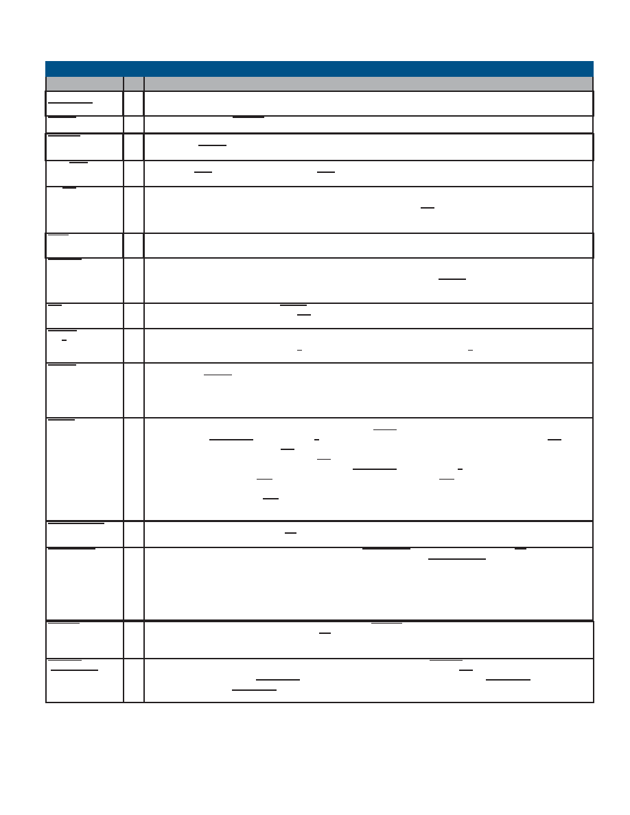
Memory Write or Zero Wait State. In transparent mode, active low output signal (MEMWR) will be asserted low during memo-
ry write transfers to strobe data into internal or external RAM (normally connected to the WR signal on external RAM chips).
In buffered mode, input signal (ZERO WAIT) will be used to select between the zero wait mode (ZERO WAIT= logic 0) and
the nonzero wait mode (ZERO WAIT = logic 1).
30
MEMWR (O)
/ZERO_WAIT (I)
Memory Output Enable or Address Latch. In transparent mode, MEMOE output will be used to enable data outputs for exter-
nal RAM read cycles (normally connected to the OE signal on external RAM chips). In buffered mode, ADDR_LAT input will
be used to configure the internal address latches in latched mode (when low) or transparent mode (when high).
29
MEMOE (O)/
ADDR_LAT (I)
Memory Enable Input or Trigger Select. In transparent mode, MEMENA_IN is an active low Chip Select (CS) input to the 16K
x 16 of internal shared RAM. When only using internal RAM, connect directly to MEMENA_OUT or ground. In 8-bit buffered
mode, the input signal (TRIGGER_SEL) indicates the order of byte pairs transferred to or from the BU-63825 by the host
processor. This signal has no operation (can be N/C) in the 16-bit buffered mode. In the 8-bit buffered mode, TRIGGER_SEL
should be asserted high (logic 1) if the byte order for both read operations and write operations is MSB followed by LSB.
TRIGGER_SEL should be asserted low (logic 0) if the byte order for both read operations and write operations is LSB fol-
lowed by MSB.
33
MEMENA-IN (I)
/TRIGGER_SEL (I)
Memory Enable Output. Asserted low during both host processor and 1553 protocol/memory management memory transfer
cycles. Used as a memory chip select (CS) signal for external RAM in the transparent mode.
28
MEMENA-OUT (O)
Data Transfer Acknowledge or Polarity Select. In transparent mode, active low output signal used to indicate acceptance of
the processor interface bus in response to a data transfer grant (DTGR). In 16-bit buffered mode
(TRANSPARENT/BUFFERED = logic 0 and 16/8 = logic 1), input signal used to control the logic sense of the RD/WR signal.
When POLARITY_SEL is logic 1, RD/WR must be asserted high (logic 1) for a read operation and low (logic 0) for a write
operation. When POLARITY_SEL is logic 0, RD/WR must be asserted low (logic 0) for a read operation and high (logic 1) for
a write operation. In 8-bit buffered mode (TRANSPARENT/BUFFERED = logic 0 and 16/8 = logic 0), input signal used to con-
trol the logic sense of the MSB/LSB signal. When POLARITY_SEL is logic 0, MSB/LSB must be asserted low (logic 0) to indi-
cate the transfer of the least significant byte and high (logic 1) to indicate the transfer of the most significant byte. When
POLARITY_SEL is logic 1, MSB/LSB must be asserted high (logic 1) to indicate the transfer of the least significant byte and
low (logic 0) to indicate the transfer of the most significant byte.
32
DTACK (O)/
POLARITY_SEL (I)
Data Transfer Grant or Most Significant Byte/Least Significant Byte. In transparent mode, active low input signal asserted, in
response to the DTREQ output, to indicate that access to the processor buses has been granted to the BU-63825. In 8-bit
buffered mode, input signal used to indicate which byte is being transferred (MSB or LSB). The POLARITY_SEL input con-
trols the logic sense of MSB/LSB. (Note: only the 8-bit buffered mode uses MSB/LSB.) See description of POLARITY_SEL
signal.
26
DTGRT (I)
/MSB/LSB (I)
Data Transfer Request or 16-bit/8-bit Transfer Mode Select. In transparent mode, active low output signal used to request
access to the processor interface bus (address, data, and control buses). In buffered mode, input signal used to select
between the 16-bit data transfer mode (16/8 = logic 1) and the 8 bit data transfer mode (16/8 = logic 0).
31
DTREQ (O)
/16/8 (I)
Interrupt request output. If the LEVEL/PULSE interrupt bit (bit 3) of Configuration Register #2 is low, a negative pulse of
approximately 500 ns in width is output on INT. If bit 3 is high, a low level interrupt request output will be asserted on INT.
65
INT (O)
Handshake output to host processor. For a nonzero wait state read access, signals that data is available to be read on D15
through D0. For a nonzero wait state write cycle, signals the completion of data transfer to a register or RAM location. In the
buffered zero wait state mode, active high output signal (following the rising edge of STRBD used to indicate the latching of
address and data (write only) and that an internal transfer between the address/data latches and the RAM/registers is on-going.
66
READYD (O)
Tri-state control for external address and data buffers. Generally not needed in the buffered mode. When low, external buffers
should be enabled to allow the host processor access to the BU-63825’s RAM and registers.
67
IOEN (O)
Read/Write. For host processor access, selects either reading or writing. In the 16-bit buffered mode, if polarity select is logic
(0), then RD/WR is low (logic 0 ) for read accesses and high (logic 1) for write accesses. If polarity select is logic 1 or the con-
figuration of the interface is a mode other than 16-bit buffered mode, then RD/WR is high (logic 1 ) for read accesses and low
(logic 0) for write accesses.
6
RD/WR (I)
Memory/Register. Generally connected to either a CPU address line or address decoder output. Selects between memory
access MEM/REG = 1 (or register access MEM/REG = 0 ).
5
MEM/REG (I)
Generally connected to a CPU address decoder output to select the BU-63825 for a transfer to/from either RAM or register.
May be tied to STRBD
3
SELECT (I)
Strobe Data. Used with SELECT to initiate and control the data transfer cycle between the host processor and the BU-63825.
4
STRBD (I)
Used to select between the Transparent/ DMA mode (when strapped to logic 1) and the Buffered mode (when strapped to
logic 0) for the host processor interface.
64
TRANSPARENT/
BUFFERED (I)
DESCRIPTION
PIN
SIGNAL NAME
TABLE 35. SIGNAL DESCRIPTIONS, PROCESSOR/MEMORY INTERFACE AND CONTROL (15)
相关PDF资料 |
PDF描述 |
|---|---|
| BU-63825D1-200 | 2 CHANNEL(S), 1M bps, MIL-STD-1553 CONTROLLER, CQIP70 |
| BU-63825D1-201 | 2 CHANNEL(S), 1M bps, MIL-STD-1553 CONTROLLER, CQIP70 |
| BU-63825D2-190 | 2 CHANNEL(S), 1M bps, MIL-STD-1553 CONTROLLER, CQIP70 |
| BU-63825D2-200 | 2 CHANNEL(S), 1M bps, MIL-STD-1553 CONTROLLER, CQIP70 |
| BU-63825D2-300 | 2 CHANNEL(S), 1M bps, MIL-STD-1553 CONTROLLER, CQIP70 |
相关代理商/技术参数 |
参数描述 |
|---|---|
| BU-63-9 | 功能描述:测试电夹 White Insul Alligato RoHS:否 制造商:Pomona Electronics 类型:Minigrabber clip 颜色:Black |
| BU-63C-0 | 功能描述:测试电夹 Black Insul Alligato RoHS:否 制造商:Pomona Electronics 类型:Minigrabber clip 颜色:Black |
| BU-63C-2 | 功能描述:测试电夹 Red Insul Alligator RoHS:否 制造商:Pomona Electronics 类型:Minigrabber clip 颜色:Black |
| BU-63C-4 | 功能描述:测试电夹 Yellow Insul Alligat RoHS:否 制造商:Pomona Electronics 类型:Minigrabber clip 颜色:Black |
| BU-63C-5 | 功能描述:测试电夹 Green Insul Alligato RoHS:否 制造商:Pomona Electronics 类型:Minigrabber clip 颜色:Black |
发布紧急采购,3分钟左右您将得到回复。