参数资料
| 型号: | BU4S11G2-TR |
| 厂商: | Rohm Semiconductor |
| 文件页数: | 8/14页 |
| 文件大小: | 0K |
| 描述: | IC GATE NAND SGL 2INPUT SSOP5 |
| 标准包装: | 1 |
| 系列: | 4S |
| 逻辑类型: | 与非门 |
| 电路数: | 1 |
| 输入数: | 2 |
| 电源电压: | 3 V ~ 16 V |
| 电流 - 静态(最大值): | 1µA |
| 输出电流高,低: | 3.4mA,3.4mA |
| 逻辑电平 - 低: | 1.5 V ~ 4 V |
| 逻辑电平 - 高: | 3.5 V ~ 11 V |
| 额定电压和最大 CL 时的最大传播延迟: | 30ns @ 15V,50pF |
| 工作温度: | -40°C ~ 85°C |
| 安装类型: | 表面贴装 |
| 供应商设备封装: | 5-SSOP |
| 封装/外壳: | 6-TFSOP(0.063",1.60mm 宽),5 引线 |
| 包装: | 标准包装 |
| 其它名称: | BU4S11G2-DKR BU4S11G2-DKR-ND BU4S11G2DKR |
1995 Fairchild Semiconductor Corporation
www.fairchildsemi.com
74LCX540
—
Lo
w
V
olta
g
e
Octal
Buff
er/Line
Driver
with
5V
T
olerant
Inputs
and
Outputs
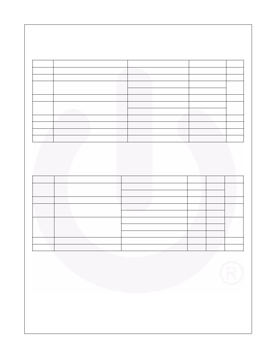
Absolute Maximum Ratings
Stresses exceeding the absolute maximum ratings may damage the device. The device may not function or be
operable above the recommended operating conditions and stressing the parts to these levels is not recommended.
In addition, extended exposure to stresses above the recommended operating conditions may affect device reliability.
The absolute maximum ratings are stress ratings only.
Recommended Operating Conditions(4)
The Recommended Operating Conditions table defines the conditions for actual device operation. Recommended
operating conditions are specified to ensure optimal performance to the datasheet specifications. Fairchild does not
recommend exceeding them or designing to absolute maximum ratings.
Notes:
3. IO Absolute Maximum Rating must be observed.
4. Unused inputs or I/O’s must be held HIGH or LOW. They may not float.
Symbol
Parameter
Conditions
Value
Units
VCC
Supply Voltage
–0.5 to +7.0
V
VI
DC Input Voltage
–0.5 to +7.0
V
VO
DC Output Voltage
Output in 3-STATE
–0.5 to +7.0
V
Output in HIGH or LOW State(3)
–0.5 to VCC + 0.5
IIK
DC Input Diode Current
VI < GND
–50
mA
IOK
DC Output Diode Current
VO < GND
–50
mA
VO > VCC
+50
IO
DC Output Source/Sink Current
±50
mA
ICC
DC Supply Current per Supply Pin
±100
mA
IGND
DC Ground Current per Ground Pin
±100
mA
TSTG
Storage Temperature
–65 to +150
°C
Symbol
Parameter
Conditions
Min.
Max.
Units
VCC
Supply Voltage
Operating
2.0
3.6
V
Data Retention
1.5
3.6
VI
Input Voltage
0
5.5
V
VO
Output Voltage
HIGH or LOW State
0
VCC
V
3-STATE
0
5.5
IOH / IOL
Output Current
VCC = 3.0V – 3.6V
±24
mA
VCC = 2.7V – 3.0V
±12
VCC = 2.3V – 2.7V
±8
TA
Free-Air Operating Temperature
–40
85
°C
t/V
Input Edge Rate
VIN = 0.8V – 2.0V, VCC = 3.0V
0
10
ns /V
74LCX540 Rev. 1.7.1
3
相关PDF资料 |
PDF描述 |
|---|---|
| SY88943VKC | IC AMP POST LIMIT 5V/3.3V 10MSOP |
| VE-2T0-IV-F2 | CONVERTER MOD DC/DC 5V 150W |
| LTC1650ACS | IC D/A CONV 16BIT R-R 16-SOIC |
| DAC312FR | IC DAC 12BIT MULT HS 20-CDIP |
| VE-2T4-IV-F2 | CONVERTER MOD DC/DC 48V 150W |
相关代理商/技术参数 |
参数描述 |
|---|---|
| BU4S584 | 制造商:ROHM Semiconductor 功能描述:SMP5 SM IC-CMOS LOGIC SCHMITT TRIGGER SINGLE 制造商:ROHM Semiconductor 功能描述:SMP5 SM IC-CMOS LOGIC SCHMITT TRIGGER SINGLE - free partial T/R at 500. |
| BU4S584G2 | 制造商:ROHM 制造商全称:Rohm 功能描述:Single Schmitt inverter |
| BU4S584G2-TL | 功能描述:变换器 INVRTR SCHMITT TRGGR 1-ELEMENT 5PIN RoHS:否 制造商:NXP Semiconductors 电路数量:6 逻辑系列:74ABT 逻辑类型:BiCMOS 高电平输出电流:- 15 mA 低电平输出电流:20 mA 传播延迟时间:2.2 ns 电源电压-最大:5.5 V 电源电压-最小:4.5 V 最大工作温度:+ 85 C 最小工作温度:- 40 C 工作温度范围: 封装 / 箱体:DIP-14 封装:Tube |
| BU4S584-G2TR | 制造商:ROHM Semiconductor 功能描述: |
| BU4S584G2-TR | 功能描述:变换器 IC SCHMITT TRIGGER SINGLE RoHS:否 制造商:NXP Semiconductors 电路数量:6 逻辑系列:74ABT 逻辑类型:BiCMOS 高电平输出电流:- 15 mA 低电平输出电流:20 mA 传播延迟时间:2.2 ns 电源电压-最大:5.5 V 电源电压-最小:4.5 V 最大工作温度:+ 85 C 最小工作温度:- 40 C 工作温度范围: 封装 / 箱体:DIP-14 封装:Tube |
发布紧急采购,3分钟左右您将得到回复。