- 您现在的位置:买卖IC网 > PDF目录298892 > BX80526F850256E (INTEL CORP) 32-BIT, 850 MHz, MICROPROCESSOR, PPGA370 PDF资料下载
参数资料
| 型号: | BX80526F850256E |
| 厂商: | INTEL CORP |
| 元件分类: | 微控制器/微处理器 |
| 英文描述: | 32-BIT, 850 MHz, MICROPROCESSOR, PPGA370 |
| 封装: | FCPGA2-370 |
| 文件页数: | 13/94页 |
| 文件大小: | 1014K |
| 代理商: | BX80526F850256E |
第1页第2页第3页第4页第5页第6页第7页第8页第9页第10页第11页第12页当前第13页第14页第15页第16页第17页第18页第19页第20页第21页第22页第23页第24页第25页第26页第27页第28页第29页第30页第31页第32页第33页第34页第35页第36页第37页第38页第39页第40页第41页第42页第43页第44页第45页第46页第47页第48页第49页第50页第51页第52页第53页第54页第55页第56页第57页第58页第59页第60页第61页第62页第63页第64页第65页第66页第67页第68页第69页第70页第71页第72页第73页第74页第75页第76页第77页第78页第79页第80页第81页第82页第83页第84页第85页第86页第87页第88页第89页第90页第91页第92页第93页第94页
20
Datasheet
Pentium III Processor for the PGA370 Socket at 500 MHz to 1.13 GHz
Note:
References to BCLK throughout this document will also imply to its complement signal, BCLK#,
in differential implementations and when noted otherwise.
For a differential clock input, all AGTL system bus timing parameters are specified with respect to
the crossing point of the rising edge of the BCLK input and the falling edge of the BCLK# input.
See the P6 Family of Processors Hardware Developer's Manual for further details.
Note:
For differential clocking, the reference voltage of the BCLK in the P6 Family of Processors
Hardware Developer's Manual is re-defined as the crossing point of the BCLK and the BCLK#
inputs.
2.5.1
Mixing Processors of Different Frequencies
In two-way MP (multi-processor) systems, mixing processors of different internal clock
frequencies is not supported and has not been validated. Pentium III processors do not support a
variable multiplier ratio; therefore, adjusting the ratio setting to a common clock frequency is not
valid. However, mixing processors of the same frequency but of different steppings is supported.
Details on support for mixed steppings is provided in the Pentium
III Processor Specification
Update.
Note:
Not all Pentium III processors for the PGA370 socket are validated for use in dual processor (DP)
systems. Refer to the Pentium III Processor Specification Update to determine which processors
are DP capable.
2.6
Voltage Identification
There are four voltage identification pins on the PGA370 socket. These pins can be used to support
automatic selection of VCCCORE voltages. These pins are not signals, but are either an open circuit
or a short circuit to VSS on the processor. The combination of opens and shorts defines the voltage
required by the processor core. The VID pins are needed to cleanly support voltage specification
variations on current and future processors. VID[3:0] are defined in Table 2.A‘1’inthis table
refers to an open pin and a ‘0’ refers to a short to ground. The voltage regulator or VRM must
supply the voltage that is requested or disable itself.
To ensure a system is ready for current and future processors, the range of values in bold in Table 2
should be supported. A smaller range will risk the ability of the system to migrate to a higher
performance processor and/or maintain compatibility with current processors.
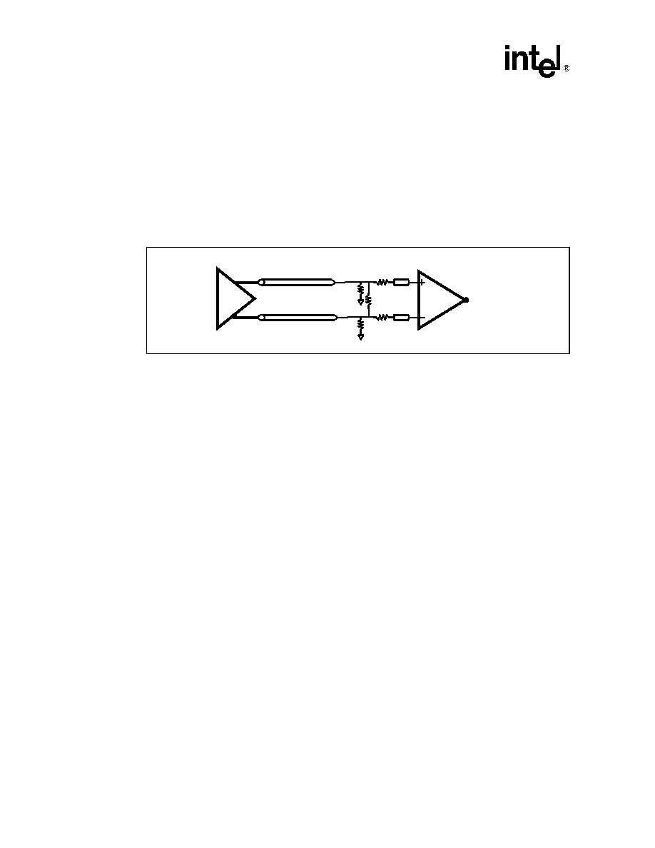
Figure 6. Differential Clocking Example
BCLK
BCLK#
Clock
Driver
Processor or
Chipset
相关PDF资料 |
PDF描述 |
|---|---|
| BX80526C866256E | 32-BIT, 866 MHz, MICROPROCESSOR, PPGA370 |
| BX80526F733256E | 32-BIT, 733 MHz, MICROPROCESSOR, PPGA370 |
| BX80547RE2533CN | 32-BIT, 2530 MHz, MICROPROCESSOR, PBGA775 |
| BX80547RE2667CN | 32-BIT, 2600 MHz, MICROPROCESSOR, PBGA775 |
| B80547RE072256 | 32-BIT, 2800 MHz, MICROPROCESSOR, PBGA775 |
相关代理商/技术参数 |
参数描述 |
|---|---|
| BX80526H800256E827304 | 制造商:Intel 功能描述:MPU PENTIUM III CISC 64BIT 0.18UM 800MHZ 370PIN FCPGA - Boxed Product (Development Kits) |
| BX80526KY7002M | 制造商:Intel 功能描述:MPU PENTIUM III XEON 64-BIT 0.18UM 700MHZ - Boxed Product (Development Kits) |
| BX80526KY9002M | 制造商:Intel 功能描述:MPU PENTIUM III XEON 64-BIT 0.18UM 900MHZ - Boxed Product (Development Kits) |
| BX80528JK150GR | 制造商:未知厂家 制造商全称:未知厂家 功能描述:Microprocessor |
| BX80528JK150GR2 | 制造商:未知厂家 制造商全称:未知厂家 功能描述:Microprocessor |
发布紧急采购,3分钟左右您将得到回复。