- 您现在的位置:买卖IC网 > PDF目录3809 > C8051F020 (Silicon Laboratories Inc)IC 8051 MCU 64K FLASH 100TQFP PDF资料下载
参数资料
| 型号: | C8051F020 |
| 厂商: | Silicon Laboratories Inc |
| 文件页数: | 228/272页 |
| 文件大小: | 0K |
| 描述: | IC 8051 MCU 64K FLASH 100TQFP |
| 标准包装: | 90 |
| 系列: | C8051F02x |
| 核心处理器: | 8051 |
| 芯体尺寸: | 8-位 |
| 速度: | 25MHz |
| 连通性: | EBI/EMI,SMBus(2 线/I²C),SPI,UART/USART |
| 外围设备: | 欠压检测/复位,POR,PWM,温度传感器,WDT |
| 输入/输出数: | 64 |
| 程序存储器容量: | 64KB(64K x 8) |
| 程序存储器类型: | 闪存 |
| RAM 容量: | 4.25K x 8 |
| 电压 - 电源 (Vcc/Vdd): | 2.7 V ~ 3.6 V |
| 数据转换器: | A/D 8x8b,8x12b; D/A 2x12b |
| 振荡器型: | 内部 |
| 工作温度: | -40°C ~ 85°C |
| 封装/外壳: | 100-TQFP |
| 包装: | 托盘 |
第1页第2页第3页第4页第5页第6页第7页第8页第9页第10页第11页第12页第13页第14页第15页第16页第17页第18页第19页第20页第21页第22页第23页第24页第25页第26页第27页第28页第29页第30页第31页第32页第33页第34页第35页第36页第37页第38页第39页第40页第41页第42页第43页第44页第45页第46页第47页第48页第49页第50页第51页第52页第53页第54页第55页第56页第57页第58页第59页第60页第61页第62页第63页第64页第65页第66页第67页第68页第69页第70页第71页第72页第73页第74页第75页第76页第77页第78页第79页第80页第81页第82页第83页第84页第85页第86页第87页第88页第89页第90页第91页第92页第93页第94页第95页第96页第97页第98页第99页第100页第101页第102页第103页第104页第105页第106页第107页第108页第109页第110页第111页第112页第113页第114页第115页第116页第117页第118页第119页第120页第121页第122页第123页第124页第125页第126页第127页第128页第129页第130页第131页第132页第133页第134页第135页第136页第137页第138页第139页第140页第141页第142页第143页第144页第145页第146页第147页第148页第149页第150页第151页第152页第153页第154页第155页第156页第157页第158页第159页第160页第161页第162页第163页第164页第165页第166页第167页第168页第169页第170页第171页第172页第173页第174页第175页第176页第177页第178页第179页第180页第181页第182页第183页第184页第185页第186页第187页第188页第189页第190页第191页第192页第193页第194页第195页第196页第197页第198页第199页第200页第201页第202页第203页第204页第205页第206页第207页第208页第209页第210页第211页第212页第213页第214页第215页第216页第217页第218页第219页第220页第221页第222页第223页第224页第225页第226页第227页当前第228页第229页第230页第231页第232页第233页第234页第235页第236页第237页第238页第239页第240页第241页第242页第243页第244页第245页第246页第247页第248页第249页第250页第251页第252页第253页第254页第255页第256页第257页第258页第259页第260页第261页第262页第263页第264页第265页第266页第267页第268页第269页第270页第271页第272页
C8051F022/3
Rev. 1.4
59
6.
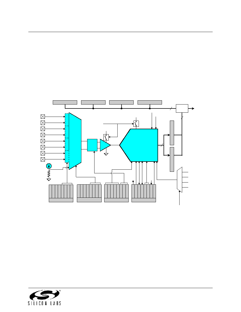
ADC0 (10-BIT ADC, C8051F022/3 ONLY)
The ADC0 subsystem for the C8051F022/3 consists of a 9-channel, configurable analog multiplexer (AMUX0), a
programmable gain amplifier (PGA0), and a 100 ksps, 10-bit successive-approximation-register ADC with integrated
track-and-hold and Programmable Window Detector (see block diagram in Figure 6.1). The AMUX0, PGA0, Data
Conversion Modes, and Window Detector are all configurable under software control via the Special Function Regis-
ters shown in Figure 6.1. The voltage reference used by ADC0 is selected as described in Section “9. VOLTAGE
REFERENCE (C8051F020/2)” on page 91 for C8051F020/2 devices, or Section “10. VOLTAGE REFERENCE
(C8051F021/3)” on page 93 for C8051F021/3 devices. The ADC0 subsystem (ADC0, track-and-hold and PGA0) is
enabled only when the AD0EN bit in the ADC0 Control register (ADC0CN) is set to logic 1. The ADC0 subsystem is
in low power shutdown when this bit is logic 0.
6.1.
Analog Multiplexer and PGA
Eight of the AMUX channels are available for external measurements while the ninth channel is internally connected
to an on-chip temperature sensor (temperature transfer function is shown in Figure 6.2). AMUX input pairs can be
programmed to operate in either differential or single-ended mode. This allows the user to select the best measure-
ment technique for each input channel, and even accommodates mode changes "on-the-fly". The AMUX defaults to
all single-ended inputs upon reset. There are two registers associated with the AMUX: the Channel Selection register
AMX0SL (Figure 6.6), and the Configuration register AMX0CF (Figure 6.7). The table in Figure 6.6 shows AMUX
functionality by channel, for each possible configuration. The PGA amplifies the AMUX output signal by an amount
determined by the states of the AMP0GN2-0 bits in the ADC0 Configuration register, ADC0CF (Figure 6.7). The
PGA can be software-programmed for gains of 0.5, 2, 4, 8 or 16. Gain defaults to unity on reset.
10-Bit
SAR
ADC
REF
+
-
AV+
TEMP
SENSOR
10
+
-
+
-
+
-
9-to-1
AMUX
(SE or
DIFF)
AV+
20
10
AD0EN
SYSC
L
K
+
-
X
AIN0
AIN1
AIN2
AIN3
AIN4
AIN5
AIN6
AIN7
Start Conversion
AGND
AD
C0
L
ADC0
H
ADC0LTL
ADC0LTH
ADC0GTL
ADC0GTH
AD0CM
Timer 3 Overflow
Timer 2 Overflow
00
01
10
11
AD0BUSY (W)
CNVSTR
AD0WINT
Comb.
Logic
AMX0SL
AM
X0AD
0
AM
X0AD
1
AM
X0AD
2
AM
X0AD
3
AMX0CF
AIN01IC
AIN23IC
AIN45IC
AIN67IC
ADC0CF
AM
P0GN0
AM
P0GN1
AM
P0GN2
AD0SC
0
AD0SC
1
AD0SC
2
AD0SC
3
AD0SC
4
ADC0CN
AD0LJST
AD0W
IN
T
AD0CM
0
AD0CM
1
AD
0BUS
Y
AD0INT
AD0TM
AD0EN
AD0CM
Figure 6.1. 10-Bit ADC0 Functional Block Diagram
相关PDF资料 |
PDF描述 |
|---|---|
| C8051F016 | IC 8051 MCU 32K FLASH 48TQFP |
| C8051F015 | IC 8051 MCU 32K FLASH 64TQFP |
| C8051F236 | IC 8051 MCU 8K FLASH 48TQFP |
| PIC14000-04I/SP | IC MCU OTP 4KX14 A/D 28DIP |
| C8051F231 | IC 8051 MCU 8K FLASH 32LQFP |
相关代理商/技术参数 |
参数描述 |
|---|---|
| C8051F020DK | 功能描述:开发板和工具包 - 8051 Dev Kit - C8051F020 21 22 23 MCUs RoHS:否 制造商:Silicon Labs 产品:Development Kits 工具用于评估:C8051F960, Si7005 核心: 接口类型:USB 工作电源电压: |
| C8051F020DK-A | 功能描述:DEV KIT FOR F020/F021/F022/F023 RoHS:否 类别:编程器,开发系统 >> 过时/停产零件编号 系列:- 标准包装:1 系列:- 类型:MCU 适用于相关产品:Freescale MC68HC908LJ/LK(80-QFP ZIF 插口) 所含物品:面板、缆线、软件、数据表和用户手册 其它名称:520-1035 |
| C8051F020DK-B | 功能描述:DEV KIT FOR F020/F021/F022/F023 RoHS:否 类别:编程器,开发系统 >> 过时/停产零件编号 系列:- 标准包装:1 系列:- 类型:MCU 适用于相关产品:Freescale MC68HC908LJ/LK(80-QFP ZIF 插口) 所含物品:面板、缆线、软件、数据表和用户手册 其它名称:520-1035 |
| C8051F020DK-E | 功能描述:DEV KIT FOR F020/F021/F022/F023 RoHS:否 类别:编程器,开发系统 >> 过时/停产零件编号 系列:- 标准包装:1 系列:- 类型:MCU 适用于相关产品:Freescale MC68HC908LJ/LK(80-QFP ZIF 插口) 所含物品:面板、缆线、软件、数据表和用户手册 其它名称:520-1035 |
| C8051F020DK-H | 功能描述:DEV KIT FOR F020/F021/F022/F023 RoHS:否 类别:编程器,开发系统 >> 过时/停产零件编号 系列:- 标准包装:1 系列:- 类型:MCU 适用于相关产品:Freescale MC68HC908LJ/LK(80-QFP ZIF 插口) 所含物品:面板、缆线、软件、数据表和用户手册 其它名称:520-1035 |
发布紧急采购,3分钟左右您将得到回复。