- 您现在的位置:买卖IC网 > PDF目录11064 > C8051F021-GQR (Silicon Laboratories Inc)IC 8051 MCU 64K FLASH 64TQFP PDF资料下载
参数资料
| 型号: | C8051F021-GQR |
| 厂商: | Silicon Laboratories Inc |
| 文件页数: | 268/272页 |
| 文件大小: | 0K |
| 描述: | IC 8051 MCU 64K FLASH 64TQFP |
| 产品培训模块: | Serial Communication Overview |
| 标准包装: | 500 |
| 系列: | C8051F02x |
| 核心处理器: | 8051 |
| 芯体尺寸: | 8-位 |
| 速度: | 25MHz |
| 连通性: | EBI/EMI,SMBus(2 线/I²C),SPI,UART/USART |
| 外围设备: | 欠压检测/复位,POR,PWM,温度传感器,WDT |
| 输入/输出数: | 32 |
| 程序存储器容量: | 64KB(64K x 8) |
| 程序存储器类型: | 闪存 |
| RAM 容量: | 4.25K x 8 |
| 电压 - 电源 (Vcc/Vdd): | 2.7 V ~ 3.6 V |
| 数据转换器: | A/D 8x8b,8x12b; D/A 2x12b |
| 振荡器型: | 内部 |
| 工作温度: | -40°C ~ 85°C |
| 封装/外壳: | 64-TQFP |
| 包装: | 带卷 (TR) |
| 配用: | 336-1200-ND - DEV KIT FOR F020/F021/F022/F023 |
第1页第2页第3页第4页第5页第6页第7页第8页第9页第10页第11页第12页第13页第14页第15页第16页第17页第18页第19页第20页第21页第22页第23页第24页第25页第26页第27页第28页第29页第30页第31页第32页第33页第34页第35页第36页第37页第38页第39页第40页第41页第42页第43页第44页第45页第46页第47页第48页第49页第50页第51页第52页第53页第54页第55页第56页第57页第58页第59页第60页第61页第62页第63页第64页第65页第66页第67页第68页第69页第70页第71页第72页第73页第74页第75页第76页第77页第78页第79页第80页第81页第82页第83页第84页第85页第86页第87页第88页第89页第90页第91页第92页第93页第94页第95页第96页第97页第98页第99页第100页第101页第102页第103页第104页第105页第106页第107页第108页第109页第110页第111页第112页第113页第114页第115页第116页第117页第118页第119页第120页第121页第122页第123页第124页第125页第126页第127页第128页第129页第130页第131页第132页第133页第134页第135页第136页第137页第138页第139页第140页第141页第142页第143页第144页第145页第146页第147页第148页第149页第150页第151页第152页第153页第154页第155页第156页第157页第158页第159页第160页第161页第162页第163页第164页第165页第166页第167页第168页第169页第170页第171页第172页第173页第174页第175页第176页第177页第178页第179页第180页第181页第182页第183页第184页第185页第186页第187页第188页第189页第190页第191页第192页第193页第194页第195页第196页第197页第198页第199页第200页第201页第202页第203页第204页第205页第206页第207页第208页第209页第210页第211页第212页第213页第214页第215页第216页第217页第218页第219页第220页第221页第222页第223页第224页第225页第226页第227页第228页第229页第230页第231页第232页第233页第234页第235页第236页第237页第238页第239页第240页第241页第242页第243页第244页第245页第246页第247页第248页第249页第250页第251页第252页第253页第254页第255页第256页第257页第258页第259页第260页第261页第262页第263页第264页第265页第266页第267页当前第268页第269页第270页第271页第272页
C8051F020/1/2/3
Rev. 1.4
95
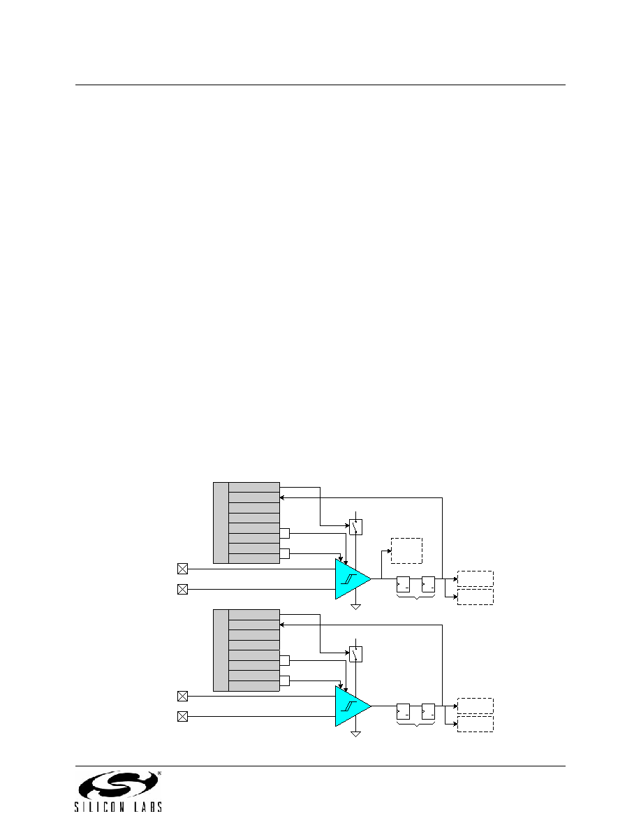
11.
COMPARATORS
Each MCU includes two on-board voltage comparators as shown in Figure 11.1. The inputs of each Comparator are
available at the package pins. The output of each comparator is optionally available at the package pins via the I/O
crossbar. When assigned to package pins, each comparator output can be programmed to operate in open drain or
push-pull modes. See Section “17. PORT INPUT/OUTPUT” on page 161 for Crossbar and port initialization
details.
The hysteresis of each comparator is software-programmable via its respective Comparator control register (CPT0CN
and CPT1CN for Comparator0 and Comparator1, respectively). The user can program both the amount of hysteresis
voltage (referred to the input voltage) and the positive and negative-going symmetry of this hysteresis around the
threshold voltage. The output of the comparator can be polled in software, or can be used as an interrupt source. Each
comparator can be individually enabled or disabled (shutdown). When disabled, the comparator output (if assigned to
a Port I/O pin via the Crossbar) defaults to the logic low state, its interrupt capability is suspended and its supply cur-
rent falls to less than 1 A. Comparator inputs can be externally driven from -0.25 V to (AV+) + 0.25 V without dam-
age or upset.
The Comparator0 hysteresis is programmed using bits 3-0 in the Comparator0 Control Register CPT0CN (shown in
Figure 11.1). The amount of negative hysteresis voltage is determined by the settings of the CP0HYN bits; In a simi-
lar way, the amount of positive hysteresis is determined by the setting the CP0HYP bits. See Table 11.1 on page 99
for hysteresis level specifications.
Comparator interrupts can be generated on rising-edge and/or falling-edge output transitions. (For interrupt enable
and priority control, see Section “12.3. Interrupt Handler” on page 116). The CP0FIF flag is set upon a
Comparator0 falling-edge interrupt, and the CP0RIF flag is set upon the Comparator0 rising-edge interrupt. Once set,
these bits remain set until cleared by software. The Output State of Comparator0 can be obtained at any time by read-
ing the CP0OUT bit. Comparator0 is enabled by setting the CP0EN bit to logic 1, and is disabled by clearing this bit
+
-
AV+
Q
SET
CLR
D
Q
SET
CLR
D
Crossbar
Interrupt
Handler
Reset
Decision
Tree
(SYNCHRONIZER)
CP0+
CP0-
AGND
CPT0C
N
CP0EN
CP0OUT
CP0RIF
CP0FIF
CP0HYP1
CP0HYP0
CP0HYN1
CP0HYN0
+
-
AV+
Q
SET
CLR
D
Q
SET
CLR
D
Crossbar
Interrupt
Handler
(SYNCHRONIZER)
CP1+
CP1-
AGND
CP
T
1C
N
CP1EN
CP1OUT
CP1RIF
CP1FIF
CP1HYP1
CP1HYP0
CP1HYN1
CP1HYN0
Figure 11.1. Comparator Functional Block Diagram
相关PDF资料 |
PDF描述 |
|---|---|
| MC74LVX8053DR2 | IC MUX/DEMUX TRIPLE 2X1 16SOIC |
| MC74LVX8051MELG | IC MUX/DEMUX 8X1 16SOEIAJ |
| MC74LVX8051MEL | IC MUX/DEMUX 8X1 16SOEIAJ |
| MC74LVX8051M | IC MUX/DEMUX 8X1 16SOEIAJ |
| MC74LVX8051DTR2 | IC MUX/DEMUX 8X1 16TSSOP |
相关代理商/技术参数 |
参数描述 |
|---|---|
| C8051F021R | 功能描述:8位微控制器 -MCU ADC 12/64Pin RoHS:否 制造商:Silicon Labs 核心:8051 处理器系列:C8051F39x 数据总线宽度:8 bit 最大时钟频率:50 MHz 程序存储器大小:16 KB 数据 RAM 大小:1 KB 片上 ADC:Yes 工作电源电压:1.8 V to 3.6 V 工作温度范围:- 40 C to + 105 C 封装 / 箱体:QFN-20 安装风格:SMD/SMT |
| C8051F022 | 功能描述:8位微控制器 -MCU 64KB 10ADC RoHS:否 制造商:Silicon Labs 核心:8051 处理器系列:C8051F39x 数据总线宽度:8 bit 最大时钟频率:50 MHz 程序存储器大小:16 KB 数据 RAM 大小:1 KB 片上 ADC:Yes 工作电源电压:1.8 V to 3.6 V 工作温度范围:- 40 C to + 105 C 封装 / 箱体:QFN-20 安装风格:SMD/SMT |
| C8051F022/0065 | 制造商:Silicon Laboratories Inc 功能描述: |
| C8051F022-GQ | 功能描述:8位微控制器 -MCU 64KB 10ADC 100P MCU RoHS:否 制造商:Silicon Labs 核心:8051 处理器系列:C8051F39x 数据总线宽度:8 bit 最大时钟频率:50 MHz 程序存储器大小:16 KB 数据 RAM 大小:1 KB 片上 ADC:Yes 工作电源电压:1.8 V to 3.6 V 工作温度范围:- 40 C to + 105 C 封装 / 箱体:QFN-20 安装风格:SMD/SMT |
| C8051F022-GQR | 功能描述:8位微控制器 -MCU 64KB 10ADC 100P MCU Tape and Reel RoHS:否 制造商:Silicon Labs 核心:8051 处理器系列:C8051F39x 数据总线宽度:8 bit 最大时钟频率:50 MHz 程序存储器大小:16 KB 数据 RAM 大小:1 KB 片上 ADC:Yes 工作电源电压:1.8 V to 3.6 V 工作温度范围:- 40 C to + 105 C 封装 / 箱体:QFN-20 安装风格:SMD/SMT |
发布紧急采购,3分钟左右您将得到回复。