- 您现在的位置:买卖IC网 > PDF目录3809 > C8051F022 (Silicon Laboratories Inc)IC 8051 MCU 64K FLASH 100TQFP PDF资料下载
参数资料
| 型号: | C8051F022 |
| 厂商: | Silicon Laboratories Inc |
| 文件页数: | 111/272页 |
| 文件大小: | 0K |
| 描述: | IC 8051 MCU 64K FLASH 100TQFP |
| 标准包装: | 90 |
| 系列: | C8051F02x |
| 核心处理器: | 8051 |
| 芯体尺寸: | 8-位 |
| 速度: | 25MHz |
| 连通性: | EBI/EMI,SMBus(2 线/I²C),SPI,UART/USART |
| 外围设备: | 欠压检测/复位,POR,PWM,温度传感器,WDT |
| 输入/输出数: | 64 |
| 程序存储器容量: | 64KB(64K x 8) |
| 程序存储器类型: | 闪存 |
| RAM 容量: | 4.25K x 8 |
| 电压 - 电源 (Vcc/Vdd): | 2.7 V ~ 3.6 V |
| 数据转换器: | A/D 8x8b,8x10b; D/A 2x12b |
| 振荡器型: | 内部 |
| 工作温度: | -40°C ~ 85°C |
| 封装/外壳: | 100-TQFP |
| 包装: | 托盘 |
第1页第2页第3页第4页第5页第6页第7页第8页第9页第10页第11页第12页第13页第14页第15页第16页第17页第18页第19页第20页第21页第22页第23页第24页第25页第26页第27页第28页第29页第30页第31页第32页第33页第34页第35页第36页第37页第38页第39页第40页第41页第42页第43页第44页第45页第46页第47页第48页第49页第50页第51页第52页第53页第54页第55页第56页第57页第58页第59页第60页第61页第62页第63页第64页第65页第66页第67页第68页第69页第70页第71页第72页第73页第74页第75页第76页第77页第78页第79页第80页第81页第82页第83页第84页第85页第86页第87页第88页第89页第90页第91页第92页第93页第94页第95页第96页第97页第98页第99页第100页第101页第102页第103页第104页第105页第106页第107页第108页第109页第110页当前第111页第112页第113页第114页第115页第116页第117页第118页第119页第120页第121页第122页第123页第124页第125页第126页第127页第128页第129页第130页第131页第132页第133页第134页第135页第136页第137页第138页第139页第140页第141页第142页第143页第144页第145页第146页第147页第148页第149页第150页第151页第152页第153页第154页第155页第156页第157页第158页第159页第160页第161页第162页第163页第164页第165页第166页第167页第168页第169页第170页第171页第172页第173页第174页第175页第176页第177页第178页第179页第180页第181页第182页第183页第184页第185页第186页第187页第188页第189页第190页第191页第192页第193页第194页第195页第196页第197页第198页第199页第200页第201页第202页第203页第204页第205页第206页第207页第208页第209页第210页第211页第212页第213页第214页第215页第216页第217页第218页第219页第220页第221页第222页第223页第224页第225页第226页第227页第228页第229页第230页第231页第232页第233页第234页第235页第236页第237页第238页第239页第240页第241页第242页第243页第244页第245页第246页第247页第248页第249页第250页第251页第252页第253页第254页第255页第256页第257页第258页第259页第260页第261页第262页第263页第264页第265页第266页第267页第268页第269页第270页第271页第272页
C8051F020/1/2/3
Rev. 1.4
199
19.2.
SPI0 Operation
Only a SPI master device can initiate a data transfer. SPI0 is placed in master mode by setting the Master Enable flag
(MSTEN, SPI0CN.1). Writing a byte of data to the SPI0 data register (SPI0DAT) when in Master Mode starts a data
transfer. The SPI0 master immediately shifts out the data serially on the MOSI line while providing the serial clock
on SCK. The SPIF (SPI0CN.7) flag is set to logic 1 at the end of the transfer. If interrupts are enabled, an interrupt
request is generated when the SPIF flag is set. The SPI0 master can be configured to shift in/out from one to eight bits
in a transfer operation in order to accommodate slave devices with different word lengths. The SPIFRS bits in the
SP0I Configuration Register (SPI0CFG.[2:0]) are used to select the number of bits to shift in/out in a transfer opera-
tion.
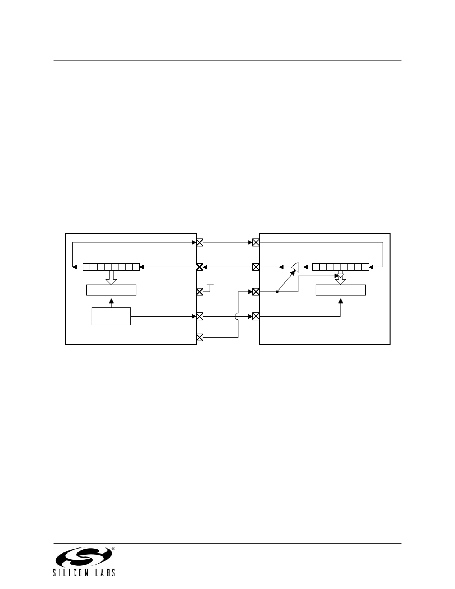
While the SPI0 master transfers data to a slave on the MOSI line, the addressed SPI slave device simultaneously
transfers the contents of its shift register to the SPI master on the MISO line in a full-duplex operation. The data byte
received from the slave replaces the data in the master's data register. Therefore, the SPIF flag serves as both a trans-
mit-complete and receive-data-ready flag. The data transfer in both directions is synchronized with the serial clock
generated by the master. Figure 19.3 illustrates the full-duplex operation of an SPI master and an addressed slave.
When SPI0 is enabled and not configured as a master, it will operate as an SPI slave. Another SPI device acting as a
master will initiate a transfer by driving the NSS input signal low. The master then shifts data out of the shift register
on the MOSI pin using the its serial clock. The SPIF flag is set to logic 1 when the NSS signal goes high, indicating
the end of a data transfer. Note that following a rising edge on NSS, the receive buffer will always contain the last
8 bits of data in the slave shift register. The slave can load its shift register for the next data transfer by writing to the
SPI0 data register. The slave must make the write to the data register at least one SPI serial clock cycle before the
master starts the next transmission. Otherwise, the byte of data already in the slave's shift register will be transferred.
Note that the NSS signal must be driven low at least 2 system clocks before the first active edge of SCK for each byte
transfer.
The SPI0 data register is double buffered on reads, but not on writes. If a write to SPI0DAT is attempted during a data
transfer, the WCOL flag (SPI0CN.6) will be set to logic 1 and the write will be ignored. The current data transfer will
continue uninterrupted. A read of the SPI0 data register by the system controller actually reads the receive buffer. The
receive overrun flag (RXOVRN in register SPI0CN) is set anytime a SPI0 slave detects a rising edge on NSS while
the receive buffer still holds unread data from a previous transfer. The new data is not transferred to the receive buf-
fer, allowing the previously received data byte to be read. The data byte causing the overrun is lost.
Figure 19.3. Full Duplex Operation
Receive Buffer
0
1
2
3
4
5
6
7
SPI SHIFT REGISTER
SLAVE DEVICE
MOSI
MISO
NSS
Receive Buffer
0
1
2
3
4
5
6
7
SPI SHIFT REGISTER
MASTER DEVICE
MOSI
MISO
NSS
VDD
Baud Rate
Generator
SCK
Px.y
相关PDF资料 |
PDF描述 |
|---|---|
| PIC32MX675F512L-80I/BG | IC MCU 32BIT 512KB FLASH 121XBGA |
| 4-100526-8 | Z-PACK F.CODING KEY |
| C8051F021 | IC 8051 MCU 64K FLASH 64TQFP |
| PIC18F4685-I/P | IC PIC MCU FLASH 48KX16 40DIP |
| C8051F020 | IC 8051 MCU 64K FLASH 100TQFP |
相关代理商/技术参数 |
参数描述 |
|---|---|
| C8051F022/0065 | 制造商:Silicon Laboratories Inc 功能描述: |
| C8051F022-GQ | 功能描述:8位微控制器 -MCU 64KB 10ADC 100P MCU RoHS:否 制造商:Silicon Labs 核心:8051 处理器系列:C8051F39x 数据总线宽度:8 bit 最大时钟频率:50 MHz 程序存储器大小:16 KB 数据 RAM 大小:1 KB 片上 ADC:Yes 工作电源电压:1.8 V to 3.6 V 工作温度范围:- 40 C to + 105 C 封装 / 箱体:QFN-20 安装风格:SMD/SMT |
| C8051F022-GQR | 功能描述:8位微控制器 -MCU 64KB 10ADC 100P MCU Tape and Reel RoHS:否 制造商:Silicon Labs 核心:8051 处理器系列:C8051F39x 数据总线宽度:8 bit 最大时钟频率:50 MHz 程序存储器大小:16 KB 数据 RAM 大小:1 KB 片上 ADC:Yes 工作电源电压:1.8 V to 3.6 V 工作温度范围:- 40 C to + 105 C 封装 / 箱体:QFN-20 安装风格:SMD/SMT |
| C8051F022R | 功能描述:8位微控制器 -MCU ADC 10/100Pin RoHS:否 制造商:Silicon Labs 核心:8051 处理器系列:C8051F39x 数据总线宽度:8 bit 最大时钟频率:50 MHz 程序存储器大小:16 KB 数据 RAM 大小:1 KB 片上 ADC:Yes 工作电源电压:1.8 V to 3.6 V 工作温度范围:- 40 C to + 105 C 封装 / 箱体:QFN-20 安装风格:SMD/SMT |
| C8051F023 | 功能描述:8位微控制器 -MCU 64KB 10ADC RoHS:否 制造商:Silicon Labs 核心:8051 处理器系列:C8051F39x 数据总线宽度:8 bit 最大时钟频率:50 MHz 程序存储器大小:16 KB 数据 RAM 大小:1 KB 片上 ADC:Yes 工作电源电压:1.8 V to 3.6 V 工作温度范围:- 40 C to + 105 C 封装 / 箱体:QFN-20 安装风格:SMD/SMT |
发布紧急采购,3分钟左右您将得到回复。