- 您现在的位置:买卖IC网 > PDF目录17087 > C8051F040-TB (Silicon Laboratories Inc)BOARD PROTOTYPING W/C8051F040 PDF资料下载
参数资料
| 型号: | C8051F040-TB |
| 厂商: | Silicon Laboratories Inc |
| 文件页数: | 8/16页 |
| 文件大小: | 0K |
| 描述: | BOARD PROTOTYPING W/C8051F040 |
| 标准包装: | 1 |
| 类型: | MCU |
| 适用于相关产品: | C8051F040 |
| 所含物品: | 板 |
�� �
�
�C8051F04x-DK�
�6.1.� System� Clock� Sources�
�The� C8051F040� device� installed� on� the� target� board� features� a� calibrated� programmable� internal� oscillator� which� is�
�enabled� as� the� system� clock� source� on� reset.� After� reset,� the� internal� oscillator� operates� at� a� frequency� of�
�3.0625� MHz� (±2%)� by� default� but� may� be� configured� by� software� to� operate� at� other� frequencies.� Therefore,� in� many�
�applications� an� external� oscillator� is� not� required.� However,� an� external� 22.1184� MHz� crystal� is� installed� on� the� target�
�board� for� additional� applications.� Refer� to� the� C8051F04x� data� sheet� for� more� information� on� configuring� the� system�
�clock� source.�
�6.2.� Switches� and� LEDs�
�Two� switches� are� provided� on� the� target� board.� Switch� SW1� is� connected� to� the� RESET� pin� of� the� C8051F040.�
�Pressing� SW1� puts� the� device� into� its� hardware-reset� state.� Switch� SW2� is� connected� to� the� C8051F040’s� general�
�purpose� I/O� (GPIO)� pin� through� headers.� Pressing� SW2� generates� a� logic� low� signal� on� the� port� pin.� Remove� the�
�shorting� block� from� the� header� to� disconnect� SW2� from� the� port� pins.� The� port� pin� signal� is� also� routed� to� a� pin� on�
�the� J24� I/O� connector.� See� Table� 1� for� the� port� pins� and� headers� corresponding� to� each� switch.�
�Two� LEDs� are� also� provided� on� the� target� board.� The� red� LED� labeled� PWR� is� used� to� indicate� a� power� connection�
�to� the� target� board.� The� green� LED� labeled� with� a� port� pin� name� is� connected� to� the� C8051F040’s� GPIO� pin�
�through� headers.� Remove� the� shorting� block� from� the� header� to� disconnect� the� LED� from� the� port� pin.� The� port� pin�
�signal� is� also� routed� to� a� pin� on� the� J24� I/O� connector.� See� Table� 1� for� the� port� pins� and� headers� corresponding� to�
�each� LED.�
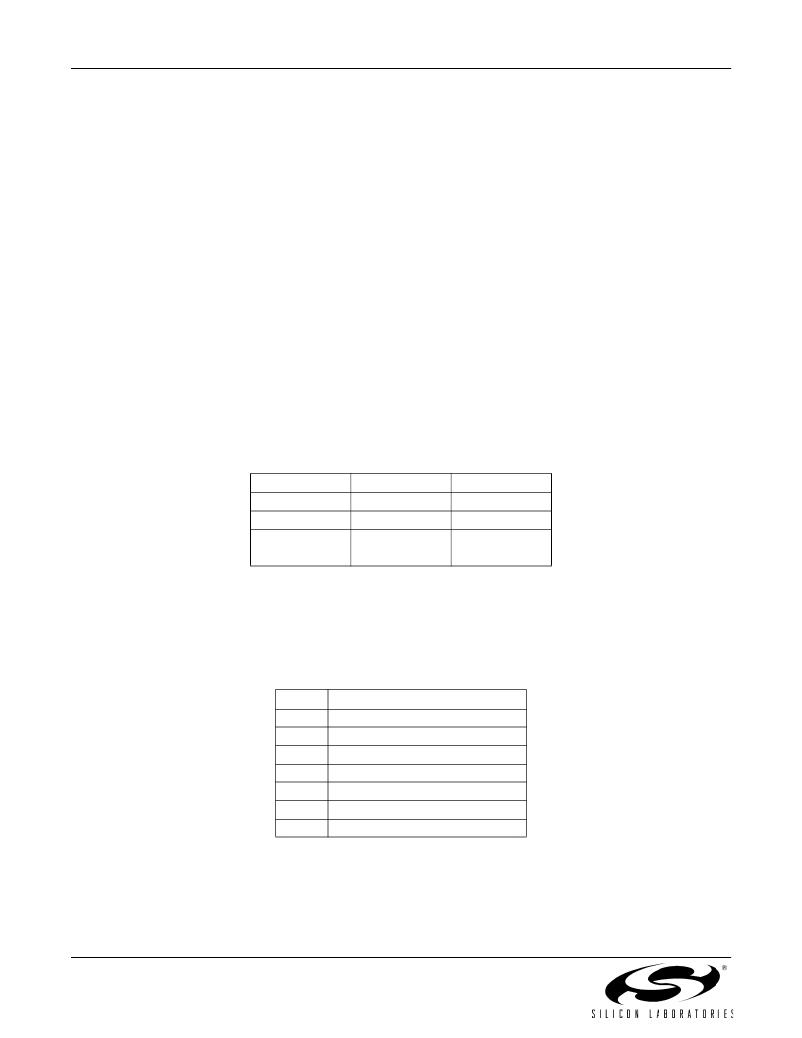
�Table� 1.� Target� Board� I/O� Descriptions�
�Description�
�SW1�
�SW2�
�Green� LED�
�Red� LED�
�I/O�
�Reset�
�P3.7�
�P1.6�
�PWR�
�Header�
�none�
�J1�
�J3�
�none�
�6.3.� Target� Board� JTAG� Interface� (J4)�
�The� JTAG� connector� (J4)� provides� access� to� the� JTAG� pins� of� the� C8051F040.� It� is� used� to� connect� the� Serial�
�Adapter� or� the� USB� Debug� Adapter� to� the� target� board� for� in-circuit� debugging� and� Flash� programming.� Table� 2�
�shows� the� JTAG� pin� definitions.�
�Table� 2.� JTAG� Connector� Pin� Descriptions�
�8�
�Pin� #�
�1�
�2,� 3,� 9�
�4�
�5�
�6�
�7�
�8,� 10�
�Description�
�+3� VD� (+3.3� VDC)�
�GND� (Ground)�
�TCK�
�TMS�
�TDO�
�TDI�
�Not� Connected�
�Rev.� 0.6�
�相关PDF资料 |
PDF描述 |
|---|---|
| HBM06DSEF-S243 | CONN EDGECARD 12POS .156 EYELET |
| SCRH105R-220 | INDUCTOR SMD 22UH 2.44A 100KHZ |
| RBC17DRYH-S13 | CONN EDGECARD 34POS .100 EXTEND |
| VI-JN0-EZ | CONVERTER MOD DC/DC 5V 25W |
| AP2141SG-13 | IC PWR SW USB 1CH 0.5A 8-SOIC |
相关代理商/技术参数 |
参数描述 |
|---|---|
| C8051F040-TB-K | 功能描述:BOARD PROTOTYPING W/C8051F040 制造商:silicon labs 系列:- 零件状态:在售 板类型:评估平台 类型:MCU 8-位 核心处理器:8051 操作系统:- 平台:- 配套使用产品/相关产品:C8051F04x 安装类型:固定 内容:板 标准包装:1 |
| C8051F041 | 功能描述:8位微控制器 -MCU 64KB 12ADC RoHS:否 制造商:Silicon Labs 核心:8051 处理器系列:C8051F39x 数据总线宽度:8 bit 最大时钟频率:50 MHz 程序存储器大小:16 KB 数据 RAM 大小:1 KB 片上 ADC:Yes 工作电源电压:1.8 V to 3.6 V 工作温度范围:- 40 C to + 105 C 封装 / 箱体:QFN-20 安装风格:SMD/SMT |
| C8051F041-GQ | 功能描述:8位微控制器 -MCU 64KB 12ADC CAN 64P MCU RoHS:否 制造商:Silicon Labs 核心:8051 处理器系列:C8051F39x 数据总线宽度:8 bit 最大时钟频率:50 MHz 程序存储器大小:16 KB 数据 RAM 大小:1 KB 片上 ADC:Yes 工作电源电压:1.8 V to 3.6 V 工作温度范围:- 40 C to + 105 C 封装 / 箱体:QFN-20 安装风格:SMD/SMT |
| C8051F041-GQR | 功能描述:8位微控制器 -MCU 64KB 12ADC CAN 64Pin Tape and Reel RoHS:否 制造商:Silicon Labs 核心:8051 处理器系列:C8051F39x 数据总线宽度:8 bit 最大时钟频率:50 MHz 程序存储器大小:16 KB 数据 RAM 大小:1 KB 片上 ADC:Yes 工作电源电压:1.8 V to 3.6 V 工作温度范围:- 40 C to + 105 C 封装 / 箱体:QFN-20 安装风格:SMD/SMT |
| C8051F041R | 功能描述:8位微控制器 -MCU ADC 12/64Pin RoHS:否 制造商:Silicon Labs 核心:8051 处理器系列:C8051F39x 数据总线宽度:8 bit 最大时钟频率:50 MHz 程序存储器大小:16 KB 数据 RAM 大小:1 KB 片上 ADC:Yes 工作电源电压:1.8 V to 3.6 V 工作温度范围:- 40 C to + 105 C 封装 / 箱体:QFN-20 安装风格:SMD/SMT |
发布紧急采购,3分钟左右您将得到回复。