- 您现在的位置:买卖IC网 > PDF目录3809 > C8051F042 (Silicon Laboratories Inc)IC 8051 MCU 64K FLASH 100TQFP PDF资料下载
参数资料
| 型号: | C8051F042 |
| 厂商: | Silicon Laboratories Inc |
| 文件页数: | 160/328页 |
| 文件大小: | 0K |
| 描述: | IC 8051 MCU 64K FLASH 100TQFP |
| 标准包装: | 90 |
| 系列: | C8051F04x |
| 核心处理器: | 8051 |
| 芯体尺寸: | 8-位 |
| 速度: | 25MHz |
| 连通性: | CAN,EBI/EMI,SMBus(2 线/I²C),SPI,UART/USART |
| 外围设备: | 欠压检测/复位,POR,PWM,温度传感器,WDT |
| 输入/输出数: | 64 |
| 程序存储器容量: | 64KB(64K x 8) |
| 程序存储器类型: | 闪存 |
| RAM 容量: | 4.25K x 8 |
| 电压 - 电源 (Vcc/Vdd): | 2.7 V ~ 3.6 V |
| 数据转换器: | A/D 8x8b,13x10b; D/A 2x10b,2x12b |
| 振荡器型: | 内部 |
| 工作温度: | -40°C ~ 85°C |
| 封装/外壳: | 100-TQFP |
| 包装: | 托盘 |
第1页第2页第3页第4页第5页第6页第7页第8页第9页第10页第11页第12页第13页第14页第15页第16页第17页第18页第19页第20页第21页第22页第23页第24页第25页第26页第27页第28页第29页第30页第31页第32页第33页第34页第35页第36页第37页第38页第39页第40页第41页第42页第43页第44页第45页第46页第47页第48页第49页第50页第51页第52页第53页第54页第55页第56页第57页第58页第59页第60页第61页第62页第63页第64页第65页第66页第67页第68页第69页第70页第71页第72页第73页第74页第75页第76页第77页第78页第79页第80页第81页第82页第83页第84页第85页第86页第87页第88页第89页第90页第91页第92页第93页第94页第95页第96页第97页第98页第99页第100页第101页第102页第103页第104页第105页第106页第107页第108页第109页第110页第111页第112页第113页第114页第115页第116页第117页第118页第119页第120页第121页第122页第123页第124页第125页第126页第127页第128页第129页第130页第131页第132页第133页第134页第135页第136页第137页第138页第139页第140页第141页第142页第143页第144页第145页第146页第147页第148页第149页第150页第151页第152页第153页第154页第155页第156页第157页第158页第159页当前第160页第161页第162页第163页第164页第165页第166页第167页第168页第169页第170页第171页第172页第173页第174页第175页第176页第177页第178页第179页第180页第181页第182页第183页第184页第185页第186页第187页第188页第189页第190页第191页第192页第193页第194页第195页第196页第197页第198页第199页第200页第201页第202页第203页第204页第205页第206页第207页第208页第209页第210页第211页第212页第213页第214页第215页第216页第217页第218页第219页第220页第221页第222页第223页第224页第225页第226页第227页第228页第229页第230页第231页第232页第233页第234页第235页第236页第237页第238页第239页第240页第241页第242页第243页第244页第245页第246页第247页第248页第249页第250页第251页第252页第253页第254页第255页第256页第257页第258页第259页第260页第261页第262页第263页第264页第265页第266页第267页第268页第269页第270页第271页第272页第273页第274页第275页第276页第277页第278页第279页第280页第281页第282页第283页第284页第285页第286页第287页第288页第289页第290页第291页第292页第293页第294页第295页第296页第297页第298页第299页第300页第301页第302页第303页第304页第305页第306页第307页第308页第309页第310页第311页第312页第313页第314页第315页第316页第317页第318页第319页第320页第321页第322页第323页第324页第325页第326页第327页第328页
C8051F040/1/2/3/4/5/6/7
242
Rev. 1.5
19.2.2. Clock Low Extension
SMBus provides a clock synchronization mechanism, similar to I2C, which allows devices with different
speed capabilities to coexist on the bus. A clock-low extension is used during a transfer in order to allow
slower slave devices to communicate with faster masters. The slave may temporarily hold the SCL line
LOW to extend the clock low period, effectively decreasing the serial clock frequency.
19.2.3. SCL Low Timeout
If the SCL line is held low by a slave device on the bus, no further communication is possible. Furthermore,
the master cannot force the SCL line high to correct the error condition. To solve this problem, the SMBus
protocol specifies that devices participating in a transfer must detect any clock cycle held low longer than
25 ms as a “timeout” condition. Devices that have detected the timeout condition must reset the communi-
cation no later than 10 ms after detecting the timeout condition.
19.2.4. SCL High (SMBus Free) Timeout
The SMBus specification stipulates that if the SCL and SDA lines remain high for more that 50 s, the bus
is designated as free. If an SMBus device is waiting to generate a Master START, the START will be gen-
erated following the bus free timeout.
19.3. SMBus Transfer Modes
The SMBus0 interface may be configured to operate as a master and/or a slave. At any particular time, the
interface will be operating in one of the following modes: Master Transmitter, Master Receiver, Slave
Transmitter, or Slave Receiver. See Table 19.1 for transfer mode status decoding using the SMB0STA sta-
tus register. The following mode descriptions illustrate an interrupt-driven SMBus0 application; SMBus0
may alternatively be operated in polled mode.
19.3.1. Master Transmitter Mode
Serial data is transmitted on SDA while the serial clock is output on SCL. SMBus0 generates a START
condition and then transmits the first byte containing the address of the target slave device and the data
direction bit. In this case the data direction bit (R/W) will be logic 0 to indicate a "WRITE" operation. The
SMBus0 interface transmits one or more bytes of serial data, waiting for an acknowledge (ACK) from the
slave after each byte. To indicate the end of the serial transfer, SMBus0 generates a STOP condition.
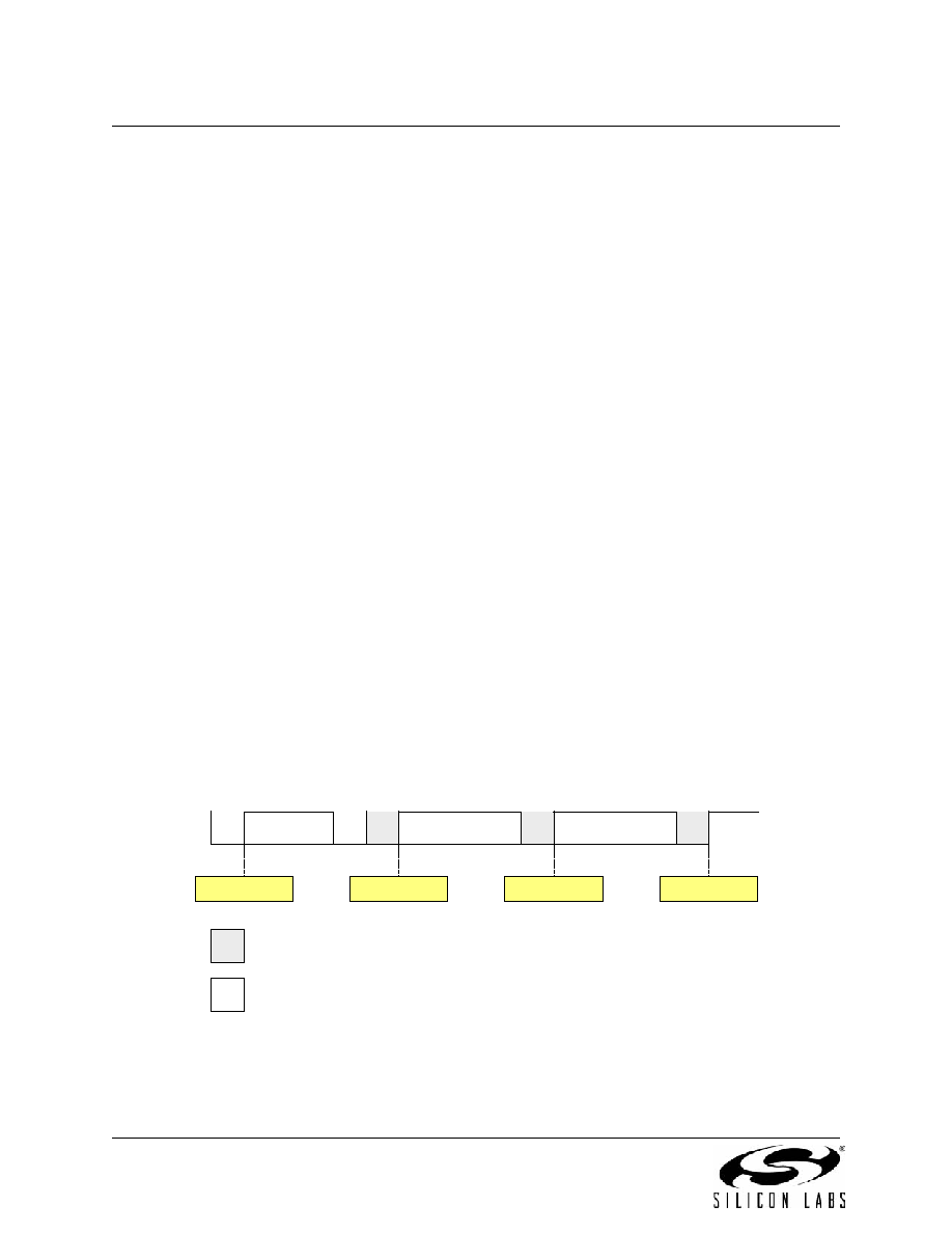
Figure 19.4. Typical Master Transmitter Sequence
A
S
W
P
Data Byte
SLA
S = START
P = STOP
A = ACK
W = WRITE
SLA = Slave Address
Received by SMBus
Interface
Transmitted by
SMBus Interface
Interrupt
相关PDF资料 |
PDF描述 |
|---|---|
| C8051F041 | IC 8051 MCU 64K FLASH 64TQFP |
| PIC18F4685-I/ML | IC PIC MCU FLASH 48KX16 44QFN |
| C8051F040 | IC 8051 MCU 64K FLASH 100TQFP |
| PIC16LF877-04I/PT | IC PIC MCU FLASH 8KX14 44TQFP |
| PIC16C64A-20I/L | IC MCU OTP 2KX14 PWM 44PLCC |
相关代理商/技术参数 |
参数描述 |
|---|---|
| C8051F042-GQ | 功能描述:8位微控制器 -MCU 64KB 10ADC CAN 100P MCU RoHS:否 制造商:Silicon Labs 核心:8051 处理器系列:C8051F39x 数据总线宽度:8 bit 最大时钟频率:50 MHz 程序存储器大小:16 KB 数据 RAM 大小:1 KB 片上 ADC:Yes 工作电源电压:1.8 V to 3.6 V 工作温度范围:- 40 C to + 105 C 封装 / 箱体:QFN-20 安装风格:SMD/SMT |
| C8051F042-GQR | 功能描述:8位微控制器 -MCU 64KB 10ADC CAN 100P Tape and Reel RoHS:否 制造商:Silicon Labs 核心:8051 处理器系列:C8051F39x 数据总线宽度:8 bit 最大时钟频率:50 MHz 程序存储器大小:16 KB 数据 RAM 大小:1 KB 片上 ADC:Yes 工作电源电压:1.8 V to 3.6 V 工作温度范围:- 40 C to + 105 C 封装 / 箱体:QFN-20 安装风格:SMD/SMT |
| C8051F042R | 功能描述:8位微控制器 -MCU ADC 10/100Pin RoHS:否 制造商:Silicon Labs 核心:8051 处理器系列:C8051F39x 数据总线宽度:8 bit 最大时钟频率:50 MHz 程序存储器大小:16 KB 数据 RAM 大小:1 KB 片上 ADC:Yes 工作电源电压:1.8 V to 3.6 V 工作温度范围:- 40 C to + 105 C 封装 / 箱体:QFN-20 安装风格:SMD/SMT |
| C8051F043 | 功能描述:8位微控制器 -MCU 64KB 10ADC RoHS:否 制造商:Silicon Labs 核心:8051 处理器系列:C8051F39x 数据总线宽度:8 bit 最大时钟频率:50 MHz 程序存储器大小:16 KB 数据 RAM 大小:1 KB 片上 ADC:Yes 工作电源电压:1.8 V to 3.6 V 工作温度范围:- 40 C to + 105 C 封装 / 箱体:QFN-20 安装风格:SMD/SMT |
| C8051F043-GQ | 功能描述:8位微控制器 -MCU 64KB 10ADC CAN 64P MCU RoHS:否 制造商:Silicon Labs 核心:8051 处理器系列:C8051F39x 数据总线宽度:8 bit 最大时钟频率:50 MHz 程序存储器大小:16 KB 数据 RAM 大小:1 KB 片上 ADC:Yes 工作电源电压:1.8 V to 3.6 V 工作温度范围:- 40 C to + 105 C 封装 / 箱体:QFN-20 安装风格:SMD/SMT |
发布紧急采购,3分钟左右您将得到回复。