- 您现在的位置:买卖IC网 > PDF目录11088 > C8051F043-GQR (Silicon Laboratories Inc)IC 8051 MCU 64K FLASH 64TQFP PDF资料下载
参数资料
| 型号: | C8051F043-GQR |
| 厂商: | Silicon Laboratories Inc |
| 文件页数: | 327/328页 |
| 文件大小: | 0K |
| 描述: | IC 8051 MCU 64K FLASH 64TQFP |
| 产品培训模块: | Serial Communication Overview |
| 标准包装: | 500 |
| 系列: | C8051F04x |
| 核心处理器: | 8051 |
| 芯体尺寸: | 8-位 |
| 速度: | 25MHz |
| 连通性: | CAN,EBI/EMI,SMBus(2 线/I²C),SPI,UART/USART |
| 外围设备: | 欠压检测/复位,POR,PWM,温度传感器,WDT |
| 输入/输出数: | 32 |
| 程序存储器容量: | 64KB(64K x 8) |
| 程序存储器类型: | 闪存 |
| RAM 容量: | 4.25K x 8 |
| 电压 - 电源 (Vcc/Vdd): | 2.7 V ~ 3.6 V |
| 数据转换器: | A/D 8x8b,13x10b; D/A 2x10b,2x12b |
| 振荡器型: | 内部 |
| 工作温度: | -40°C ~ 85°C |
| 封装/外壳: | 64-TQFP |
| 包装: | 带卷 (TR) |
| 配用: | 336-1205-ND - DEV KIT FOR F040/F041/F042/F043 |
第1页第2页第3页第4页第5页第6页第7页第8页第9页第10页第11页第12页第13页第14页第15页第16页第17页第18页第19页第20页第21页第22页第23页第24页第25页第26页第27页第28页第29页第30页第31页第32页第33页第34页第35页第36页第37页第38页第39页第40页第41页第42页第43页第44页第45页第46页第47页第48页第49页第50页第51页第52页第53页第54页第55页第56页第57页第58页第59页第60页第61页第62页第63页第64页第65页第66页第67页第68页第69页第70页第71页第72页第73页第74页第75页第76页第77页第78页第79页第80页第81页第82页第83页第84页第85页第86页第87页第88页第89页第90页第91页第92页第93页第94页第95页第96页第97页第98页第99页第100页第101页第102页第103页第104页第105页第106页第107页第108页第109页第110页第111页第112页第113页第114页第115页第116页第117页第118页第119页第120页第121页第122页第123页第124页第125页第126页第127页第128页第129页第130页第131页第132页第133页第134页第135页第136页第137页第138页第139页第140页第141页第142页第143页第144页第145页第146页第147页第148页第149页第150页第151页第152页第153页第154页第155页第156页第157页第158页第159页第160页第161页第162页第163页第164页第165页第166页第167页第168页第169页第170页第171页第172页第173页第174页第175页第176页第177页第178页第179页第180页第181页第182页第183页第184页第185页第186页第187页第188页第189页第190页第191页第192页第193页第194页第195页第196页第197页第198页第199页第200页第201页第202页第203页第204页第205页第206页第207页第208页第209页第210页第211页第212页第213页第214页第215页第216页第217页第218页第219页第220页第221页第222页第223页第224页第225页第226页第227页第228页第229页第230页第231页第232页第233页第234页第235页第236页第237页第238页第239页第240页第241页第242页第243页第244页第245页第246页第247页第248页第249页第250页第251页第252页第253页第254页第255页第256页第257页第258页第259页第260页第261页第262页第263页第264页第265页第266页第267页第268页第269页第270页第271页第272页第273页第274页第275页第276页第277页第278页第279页第280页第281页第282页第283页第284页第285页第286页第287页第288页第289页第290页第291页第292页第293页第294页第295页第296页第297页第298页第299页第300页第301页第302页第303页第304页第305页第306页第307页第308页第309页第310页第311页第312页第313页第314页第315页第316页第317页第318页第319页第320页第321页第322页第323页第324页第325页第326页当前第327页第328页
C8051F040/1/2/3/4/5/6/7
98
Rev. 1.5
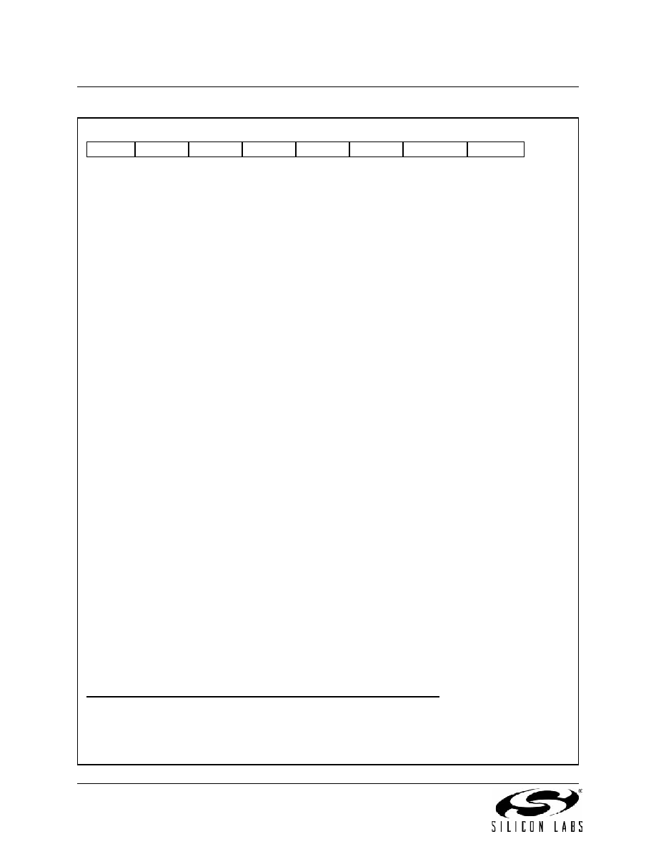
SFR Definition 7.4. ADC2CN: ADC2 Control
Bit7:
AD2EN: ADC2 Enable Bit.
0: ADC2 Disabled. ADC2 is in low-power shutdown.
1: ADC2 Enabled. ADC2 is active and ready for data conversions.
Bit6:
AD2TM: ADC2 Track Mode Bit.
0: Normal Track Mode: When ADC2 is enabled, tracking is continuous unless a conversion is in
process.
1: Low-power Track Mode: Tracking defined by AD2CM2-0 bits (see below).
Bit5:
AD2INT: ADC2 Conversion Complete Interrupt Flag.
This flag must be cleared by software.
0: ADC2 has not completed a data conversion since the last time this flag was cleared.
1: ADC2 has completed a data conversion.
Bit4:
AD2BUSY: ADC2 Busy Bit.
Read:
0: ADC2 Conversion is complete or a conversion is not currently in progress. AD2INT is set to
logic 1 on the falling edge of AD2BUSY.
1: ADC2 Conversion is in progress.
Write:
0: No Effect.
1: Initiates ADC2 Conversion if AD2CM2-0 = 000b
Bits3-1:
AD2CM2-0: ADC2 Start of Conversion Mode Select.
AD2TM = 0:
000: ADC2 conversion initiated on every write of ‘1’ to AD2BUSY.
001: ADC2 conversion initiated on overflow of Timer 3.
010: ADC2 conversion initiated on rising edge of external CNVSTR2 or CNVSTR0.
011: ADC2 conversion initiated on overflow of Timer 2.
1xx: ADC2 conversion initiated on write of ‘1’ to AD0BUSY (synchronized with ADC0 software-
commanded conversions).
AD2TM = 1:
000: Tracking initiated on write of ‘1’ to AD2BUSY and lasts 3 SAR2 clocks, followed by conver-
sion.
001: Tracking initiated on overflow of Timer 3 and lasts 3 SAR2 clocks, followed by conversion.
010: ADC2 tracks only when CNVSTR2 (or CNVSTR0, See Section 7.2.1) input is logic low; con-
version starts on rising CNVSTR2 edge.
011: Tracking initiated on overflow of Timer 2 and lasts 3 SAR2 clocks, followed by conversion.
1xx: Tracking initiated on write of ‘1’ to AD0BUSY and lasts 3 SAR2 clocks, followed by conver-
sion.
Bit0:
AD2WINT: ADC2 Window Compare Interrupt Flag.
0: ADC2 window comparison data match has not occurred since this flag was last cleared.
1: ADC2 window comparison data match has occurred. This flag must be cleared in software.
An important note about external convert start (CNVSTR0 and CNVSTR2): If CNVSTR2 is enabled in
the digital crossbar (
on page 204), CNVSTR2 will be the external convert start signal for ADC2. However, if only
CNVSTR0 is enabled in the digital crossbar and CNVSTR2 is not enabled, then CNVSTR0 may
serve as the start of conversion for both ADC0 and ADC2.
R/W
Reset Value
AD2EN
AD2TM
AD2INT AD2BUSY AD2CM2
AD2CM1
AD2CM0
AD2WINT 00000000
Bit7
Bit6
Bit5
Bit4
Bit3
Bit2
Bit1
Bit0
SFR Address:
SFR Page:
0xE8
2
相关PDF资料 |
PDF描述 |
|---|---|
| VE-B5R-IY-F4 | CONVERTER MOD DC/DC 7.5V 50W |
| MC74HC4051ADTR2 | IC MUX/DEMUX 8X1 16TSSOP |
| VE-B5R-IY-F2 | CONVERTER MOD DC/DC 7.5V 50W |
| VE-B5R-IY-F1 | CONVERTER MOD DC/DC 7.5V 50W |
| UPD78F1187AGJ-GAE-AX | MCU 16BIT 78K0R/KX3 144-LQFP |
相关代理商/技术参数 |
参数描述 |
|---|---|
| C8051F043R | 功能描述:8位微控制器 -MCU ADC 10/64Pin RoHS:否 制造商:Silicon Labs 核心:8051 处理器系列:C8051F39x 数据总线宽度:8 bit 最大时钟频率:50 MHz 程序存储器大小:16 KB 数据 RAM 大小:1 KB 片上 ADC:Yes 工作电源电压:1.8 V to 3.6 V 工作温度范围:- 40 C to + 105 C 封装 / 箱体:QFN-20 安装风格:SMD/SMT |
| C8051F044 | 功能描述:8位微控制器 -MCU 25 MIPS 64KB 10ADC RoHS:否 制造商:Silicon Labs 核心:8051 处理器系列:C8051F39x 数据总线宽度:8 bit 最大时钟频率:50 MHz 程序存储器大小:16 KB 数据 RAM 大小:1 KB 片上 ADC:Yes 工作电源电压:1.8 V to 3.6 V 工作温度范围:- 40 C to + 105 C 封装 / 箱体:QFN-20 安装风格:SMD/SMT |
| C8051F044-GQ | 功能描述:8位微控制器 -MCU 64KB 10ADC CAN 100P MCU RoHS:否 制造商:Silicon Labs 核心:8051 处理器系列:C8051F39x 数据总线宽度:8 bit 最大时钟频率:50 MHz 程序存储器大小:16 KB 数据 RAM 大小:1 KB 片上 ADC:Yes 工作电源电压:1.8 V to 3.6 V 工作温度范围:- 40 C to + 105 C 封装 / 箱体:QFN-20 安装风格:SMD/SMT |
| C8051F044-GQR | 功能描述:8位微控制器 -MCU 64KB 10ADC CAN 100P Tape and Reel RoHS:否 制造商:Silicon Labs 核心:8051 处理器系列:C8051F39x 数据总线宽度:8 bit 最大时钟频率:50 MHz 程序存储器大小:16 KB 数据 RAM 大小:1 KB 片上 ADC:Yes 工作电源电压:1.8 V to 3.6 V 工作温度范围:- 40 C to + 105 C 封装 / 箱体:QFN-20 安装风格:SMD/SMT |
| C8051F044R | 功能描述:8位微控制器 -MCU 25 MIPS 64KB 10ADC RoHS:否 制造商:Silicon Labs 核心:8051 处理器系列:C8051F39x 数据总线宽度:8 bit 最大时钟频率:50 MHz 程序存储器大小:16 KB 数据 RAM 大小:1 KB 片上 ADC:Yes 工作电源电压:1.8 V to 3.6 V 工作温度范围:- 40 C to + 105 C 封装 / 箱体:QFN-20 安装风格:SMD/SMT |
发布紧急采购,3分钟左右您将得到回复。