- 您现在的位置:买卖IC网 > PDF目录11150 > C8051F220-GQ (Silicon Laboratories Inc)IC 8051 MCU 8K FLASH 48TQFP PDF资料下载
参数资料
| 型号: | C8051F220-GQ |
| 厂商: | Silicon Laboratories Inc |
| 文件页数: | 8/146页 |
| 文件大小: | 0K |
| 描述: | IC 8051 MCU 8K FLASH 48TQFP |
| 产品培训模块: | Serial Communication Overview |
| 标准包装: | 250 |
| 系列: | C8051F2xx |
| 核心处理器: | 8051 |
| 芯体尺寸: | 8-位 |
| 速度: | 25MHz |
| 连通性: | SPI,UART/USART |
| 外围设备: | 欠压检测/复位,POR,WDT |
| 输入/输出数: | 32 |
| 程序存储器容量: | 8KB(8K x 8) |
| 程序存储器类型: | 闪存 |
| RAM 容量: | 256 x 8 |
| 电压 - 电源 (Vcc/Vdd): | 2.7 V ~ 3.6 V |
| 数据转换器: | A/D 32x8b |
| 振荡器型: | 内部 |
| 工作温度: | -40°C ~ 85°C |
| 封装/外壳: | 48-TQFP |
| 包装: | 托盘 |
| 配用: | 336-1241-ND - DEV KIT F220/221/226/230/231/236 |
| 其它名称: | 336-1238 |
第1页第2页第3页第4页第5页第6页第7页当前第8页第9页第10页第11页第12页第13页第14页第15页第16页第17页第18页第19页第20页第21页第22页第23页第24页第25页第26页第27页第28页第29页第30页第31页第32页第33页第34页第35页第36页第37页第38页第39页第40页第41页第42页第43页第44页第45页第46页第47页第48页第49页第50页第51页第52页第53页第54页第55页第56页第57页第58页第59页第60页第61页第62页第63页第64页第65页第66页第67页第68页第69页第70页第71页第72页第73页第74页第75页第76页第77页第78页第79页第80页第81页第82页第83页第84页第85页第86页第87页第88页第89页第90页第91页第92页第93页第94页第95页第96页第97页第98页第99页第100页第101页第102页第103页第104页第105页第106页第107页第108页第109页第110页第111页第112页第113页第114页第115页第116页第117页第118页第119页第120页第121页第122页第123页第124页第125页第126页第127页第128页第129页第130页第131页第132页第133页第134页第135页第136页第137页第138页第139页第140页第141页第142页第143页第144页第145页第146页
C8051F2xx
Rev. 1.6
105
14.2. General Purpose Port I/O
Each I/O port is accessed through a corresponding special function register (SFR) that is both byte
addressable and bit addressable. When writing to a port, the value written to the SFR is latched to main-
tain the output data value at each pin. When reading, the logic levels of the port’s input pins are returned
regardless of the PRTnMX settings (i.e., even when the pin is assigned to another signal by the MUX, the
Port Register can always still read its corresponding Port I/O pin), provided its pin is configured for digital
input mode. The exception to this is the execution of the read-modify-write instructions. The read-modify-
write instructions when operating on a port SFR are the following: ANL, ORL, XRL, JBC, CPL, INC, DEC,
DJNZ and MOV, CLR or SETB, when the destination is an individual bit in a port SFR. For these instruc-
tions, the value of the register (not the pin) is read, modified, and written back to the SFR.
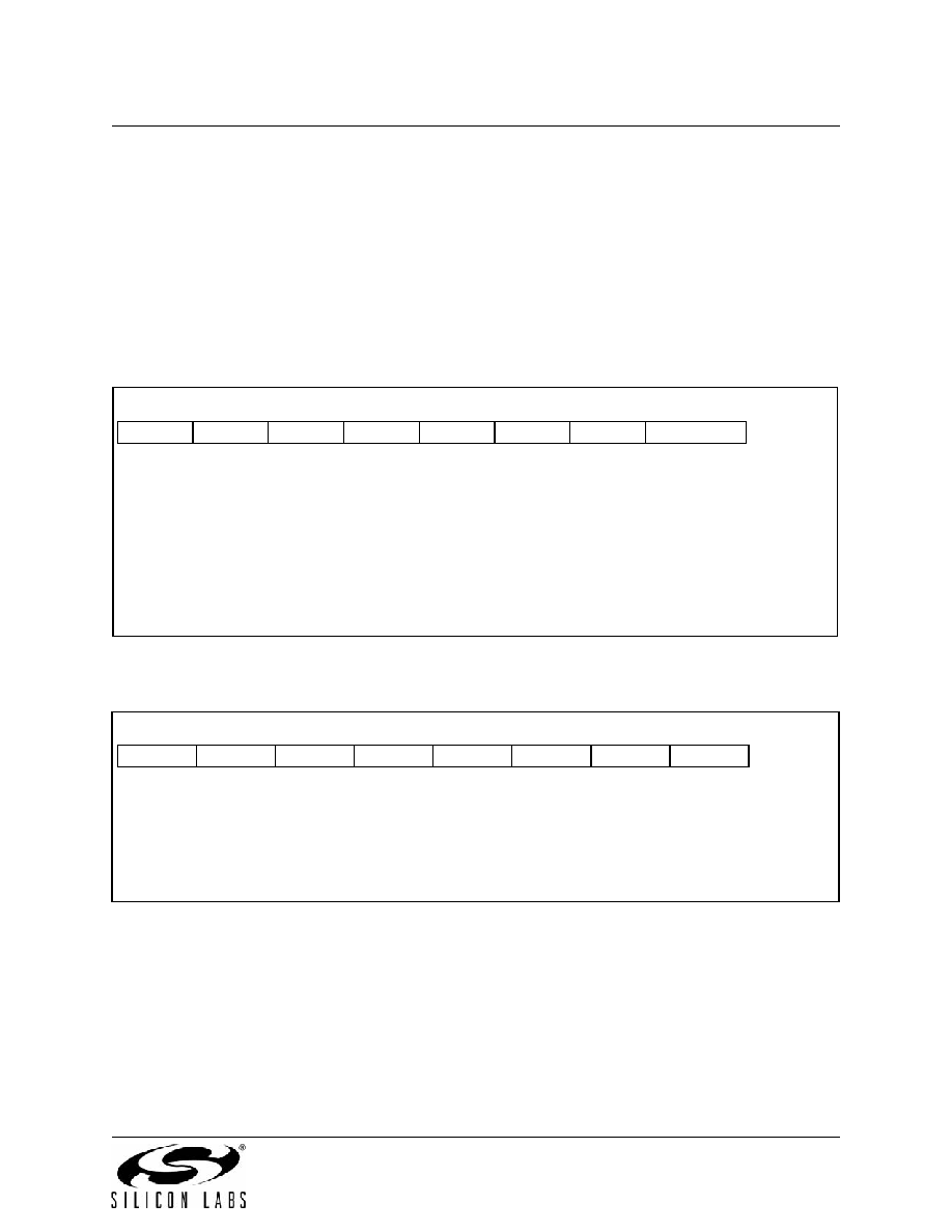
SFR Definition 14.4. P0: Port0 Register
Bits7–0: P0.[7:0]
(Write - Output appears on I/O pins per PRT0MX, PRT1MX, and PRT2MX Registers)
0: Logic Low Output.
1: Logic High Output (high impedance if corresponding PRT0CF.n bit = 0)
(Read - Regardless of PRT0MX, PRT1MX, and PRT2MX Register settings).
0: P0.n pin is logic low.
1: P0.n pin is logic high.
SFR Definition 14.5. PRT0CF: Port0 Configuration Register
Bits7–0: PRT0CF.[7:0]: Output Configuration Bits for P0.7–P0.0 (respectively)
0: Corresponding P0.n Output mode is Open-Drain.
1: Corresponding P0.n Output mode is Push-Pull.
R/W
Reset Value
P0.7
P0.6
P0.5
P0.4
P0.3
P0.2
P0.1
P0.0
11111111
Bit7
Bit6
Bit5
Bit4
Bit3
Bit2
Bit1
Bit0
SFR Address:
(bit addressable)
0x80
R/W
Reset Value
00000000
Bit7
Bit6
Bit5
Bit4
Bit3
Bit2
Bit1
Bit0
SFR Address:
0xA4
相关PDF资料 |
PDF描述 |
|---|---|
| MAX4530CWP+T | IC MULTIPLEXER 8X1 20SOIC |
| VE-213-IY-F3 | CONVERTER MOD DC/DC 24V 50W |
| VE-213-IY-F1 | CONVERTER MOD DC/DC 24V 50W |
| VE-B1N-IY-F3 | CONVERTER MOD DC/DC 18.5V 50W |
| VE-B1N-IY-F2 | CONVERTER MOD DC/DC 18.5V 50W |
相关代理商/技术参数 |
参数描述 |
|---|---|
| C8051F220-GQR | 功能描述:8位微控制器 -MCU 8KB 8ADC 48Pin MCU Tape and Reel RoHS:否 制造商:Silicon Labs 核心:8051 处理器系列:C8051F39x 数据总线宽度:8 bit 最大时钟频率:50 MHz 程序存储器大小:16 KB 数据 RAM 大小:1 KB 片上 ADC:Yes 工作电源电压:1.8 V to 3.6 V 工作温度范围:- 40 C to + 105 C 封装 / 箱体:QFN-20 安装风格:SMD/SMT |
| C8051F220R | 功能描述:8位微控制器 -MCU T-8 48 Pin RoHS:否 制造商:Silicon Labs 核心:8051 处理器系列:C8051F39x 数据总线宽度:8 bit 最大时钟频率:50 MHz 程序存储器大小:16 KB 数据 RAM 大小:1 KB 片上 ADC:Yes 工作电源电压:1.8 V to 3.6 V 工作温度范围:- 40 C to + 105 C 封装 / 箱体:QFN-20 安装风格:SMD/SMT |
| C8051F221 | 功能描述:8位微控制器 -MCU 8KB 8ADC RoHS:否 制造商:Silicon Labs 核心:8051 处理器系列:C8051F39x 数据总线宽度:8 bit 最大时钟频率:50 MHz 程序存储器大小:16 KB 数据 RAM 大小:1 KB 片上 ADC:Yes 工作电源电压:1.8 V to 3.6 V 工作温度范围:- 40 C to + 105 C 封装 / 箱体:QFN-20 安装风格:SMD/SMT |
| C8051F221-GQ | 功能描述:8位微控制器 -MCU 8KB 8ADC 32P MCU RoHS:否 制造商:Silicon Labs 核心:8051 处理器系列:C8051F39x 数据总线宽度:8 bit 最大时钟频率:50 MHz 程序存储器大小:16 KB 数据 RAM 大小:1 KB 片上 ADC:Yes 工作电源电压:1.8 V to 3.6 V 工作温度范围:- 40 C to + 105 C 封装 / 箱体:QFN-20 安装风格:SMD/SMT |
| C8051F221-GQR | 功能描述:8位微控制器 -MCU 8KB 8ADC 32Pin MCU Tape and Reel RoHS:否 制造商:Silicon Labs 核心:8051 处理器系列:C8051F39x 数据总线宽度:8 bit 最大时钟频率:50 MHz 程序存储器大小:16 KB 数据 RAM 大小:1 KB 片上 ADC:Yes 工作电源电压:1.8 V to 3.6 V 工作温度范围:- 40 C to + 105 C 封装 / 箱体:QFN-20 安装风格:SMD/SMT |
发布紧急采购,3分钟左右您将得到回复。