- 您现在的位置:买卖IC网 > PDF目录15881 > C8051F300DK-H (Silicon Laboratories Inc)DEV KIT FOR F300/301/302/304/305 PDF资料下载
参数资料
| 型号: | C8051F300DK-H |
| 厂商: | Silicon Laboratories Inc |
| 文件页数: | 7/13页 |
| 文件大小: | 0K |
| 描述: | DEV KIT FOR F300/301/302/304/305 |
| 标准包装: | 1 |
�� �
�
�C8051F30x�
�4.1.� System� Clock� Sources�
�The� C8051F300� device� installed� on� the� target� board� features� a� calibrated� programmable� internal� oscillator� which� is�
�enabled� as� the� system� clock� source� on� reset.� After� reset,� the� internal� oscillator� operates� at� a� frequency� of�
�3.0625� MHz� (+/-2%)� by� default� but� may� be� configured� by� software� to� operate� at� other� frequencies.� Therefore,� in�
�many� applications� an� external� oscillator� is� not� required.� However,� if� you� wish� to� operate� the� C8051F300� device� at� a�
�frequency� not� available� with� the� internal� oscillator,� an� external� crystal� may� be� used.� Refer� to� the� C8051F30x� data�
�sheet� for� more� information� on� configuring� the� system� clock� source.�
�The� target� board� is� designed� to� facilitate� the� installation� of� an� external� crystal.� Remove� resistors� R7� and� R8� and�
�install� the� crystal� at� the� pads� marked� Y1.� Install� a� 10� M� ?� resistor� at� R9� and� install� capacitors� at� C14� and� C15� using�
�values� appropriate� for� the� crystal� you� select.� Refer� to� the� C8051F30x� data� sheet� for� more� information� on� the� use� of�
�external� oscillators.�
�4.2.� Switches� and� LEDs�
�Two� switches� are� provided� on� the� target� board.� Switch� SW1� is� connected� to� the� RESET� pin� of� the� C8051F300.�
�Pressing� SW1� puts� the� device� into� its� hardware-reset� state.� Switch� SW2� is� connected� to� the� C8051F300’s� general�
�purpose� I/O� (GPIO)� pin� through� headers.� Pressing� SW2� generates� a� logic� low� signal� on� the� port� pin.� Remove� the�
�shorting� block� from� the� header� to� disconnect� SW2� from� the� port� pins.� The� port� pin� signal� is� also� routed� to� a� pin� on�
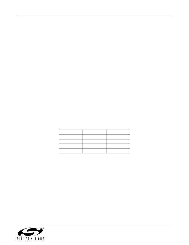
�the� J1� I/O� connector.� See� Table� 1� for� the� port� pins� and� headers� corresponding� to� each� switch.�
�Two� LEDs� are� also� provided� on� the� target� board.� The� red� LED� labeled� PWR� is� used� to� indicate� a� power� connection�
�to� the� target� board.� The� green� LED� labeled� with� a� port� pin� name� is� connected� to� the� C8051F300’s� GPIO� pin�
�through� headers.� Remove� the� shorting� block� from� the� header� to� disconnect� the� LED� from� the� port� pin.� The� port� pin�
�signal� is� also� routed� to� a� pin� on� the� J1� I/O� connector.� See� Table� 1� for� the� port� pins� and� headers� corresponding� to�
�each� LED.�
�Table� 1.� Target� Board� I/O� Descriptions�
�Description�
�SW1�
�SW2�
�Green� LED�
�Red� LED�
�I/O�
�Reset�
�P0.3�
�P0.2�
�PWR�
�Rev.� 0.6�
�Header�
�none�
�J3[3-4]�
�J3[1-2]�
�none�
�7�
�相关PDF资料 |
PDF描述 |
|---|---|
| ECC28DJXN | CONN EDGECARD 56PS .100 PRESSFIT |
| GSM10DRSN-S664 | CONN EDGECARD 20POS DIP .156 SLD |
| VI-B1W-EY-F3 | CONVERTER MOD DC/DC 5.5V 50W |
| GSM10DRSD-S664 | CONN EDGECARD 20POS DIP .156 SLD |
| VI-B1W-EY-F1 | CONVERTER MOD DC/DC 5.5V 50W |
相关代理商/技术参数 |
参数描述 |
|---|---|
| C8051F300DK-J | 功能描述:DEV KIT FOR F300/301/302/304/305 RoHS:否 类别:编程器,开发系统 >> 过时/停产零件编号 系列:- 标准包装:1 系列:- 类型:MCU 适用于相关产品:Freescale MC68HC908LJ/LK(80-QFP ZIF 插口) 所含物品:面板、缆线、软件、数据表和用户手册 其它名称:520-1035 |
| C8051F300DK-K | 功能描述:DEV KIT FOR F300/301/302/304/305 RoHS:否 类别:编程器,开发系统 >> 过时/停产零件编号 系列:- 标准包装:1 系列:- 类型:MCU 适用于相关产品:Freescale MC68HC908LJ/LK(80-QFP ZIF 插口) 所含物品:面板、缆线、软件、数据表和用户手册 其它名称:520-1035 |
| C8051F300DK-T | 功能描述:DEV KIT FOR F300/301/302/304/305 RoHS:否 类别:编程器,开发系统 >> 过时/停产零件编号 系列:- 标准包装:1 系列:- 类型:MCU 适用于相关产品:Freescale MC68HC908LJ/LK(80-QFP ZIF 插口) 所含物品:面板、缆线、软件、数据表和用户手册 其它名称:520-1035 |
| C8051F300DK-U | 功能描述:DEV KIT F300/301/302/303/304/305 RoHS:否 类别:编程器,开发系统 >> 过时/停产零件编号 系列:- 标准包装:1 系列:- 类型:MCU 适用于相关产品:Freescale MC68HC908LJ/LK(80-QFP ZIF 插口) 所含物品:面板、缆线、软件、数据表和用户手册 其它名称:520-1035 |
| C8051F300-GDI | 功能描述:8位微控制器 -MCU 8 kB Flash MCU RoHS:否 制造商:Silicon Labs 核心:8051 处理器系列:C8051F39x 数据总线宽度:8 bit 最大时钟频率:50 MHz 程序存储器大小:16 KB 数据 RAM 大小:1 KB 片上 ADC:Yes 工作电源电压:1.8 V to 3.6 V 工作温度范围:- 40 C to + 105 C 封装 / 箱体:QFN-20 安装风格:SMD/SMT |
发布紧急采购,3分钟左右您将得到回复。