- 您现在的位置:买卖IC网 > PDF目录3801 > C8051F303-GM (Silicon Laboratories Inc)IC 8051 MCU 8K FLASH 11QFN PDF资料下载
参数资料
| 型号: | C8051F303-GM |
| 厂商: | Silicon Laboratories Inc |
| 文件页数: | 115/178页 |
| 文件大小: | 0K |
| 描述: | IC 8051 MCU 8K FLASH 11QFN |
| 产品培训模块: | Serial Communication Overview |
| 标准包装: | 122 |
| 系列: | C8051F30x |
| 核心处理器: | 8051 |
| 芯体尺寸: | 8-位 |
| 速度: | 25MHz |
| 连通性: | SMBus(2 线/I²C),UART/USART |
| 外围设备: | POR,PWM,WDT |
| 输入/输出数: | 8 |
| 程序存储器容量: | 8KB(8K x 8) |
| 程序存储器类型: | 闪存 |
| RAM 容量: | 256 x 8 |
| 电压 - 电源 (Vcc/Vdd): | 2.7 V ~ 3.6 V |
| 振荡器型: | 外部 |
| 工作温度: | -40°C ~ 85°C |
| 封装/外壳: | 10-VFDFN 裸露焊盘 |
| 包装: | 管件 |
| 产品目录页面: | 623 (CN2011-ZH PDF) |
| 配用: | 336-1444-ND - ADAPTER PROGRAM TOOLSTICK F300 |
| 其它名称: | 336-1249 |
第1页第2页第3页第4页第5页第6页第7页第8页第9页第10页第11页第12页第13页第14页第15页第16页第17页第18页第19页第20页第21页第22页第23页第24页第25页第26页第27页第28页第29页第30页第31页第32页第33页第34页第35页第36页第37页第38页第39页第40页第41页第42页第43页第44页第45页第46页第47页第48页第49页第50页第51页第52页第53页第54页第55页第56页第57页第58页第59页第60页第61页第62页第63页第64页第65页第66页第67页第68页第69页第70页第71页第72页第73页第74页第75页第76页第77页第78页第79页第80页第81页第82页第83页第84页第85页第86页第87页第88页第89页第90页第91页第92页第93页第94页第95页第96页第97页第98页第99页第100页第101页第102页第103页第104页第105页第106页第107页第108页第109页第110页第111页第112页第113页第114页当前第115页第116页第117页第118页第119页第120页第121页第122页第123页第124页第125页第126页第127页第128页第129页第130页第131页第132页第133页第134页第135页第136页第137页第138页第139页第140页第141页第142页第143页第144页第145页第146页第147页第148页第149页第150页第151页第152页第153页第154页第155页第156页第157页第158页第159页第160页第161页第162页第163页第164页第165页第166页第167页第168页第169页第170页第171页第172页第173页第174页第175页第176页第177页第178页
Rev. 2.9
41
C8051F300/1/2/3/4/5
5.3.3. Settling Time Requirements
When the ADC0 input configuration is changed (i.e., a different AMUX0 or PGA selection is made), a mini-
mum tracking time is required before an accurate conversion can be performed. This tracking time is deter-
mined by the AMUX0 resistance, the ADC0 sampling capacitance, any external source resistance, and the
accuracy required for the conversion. Note that in low-power tracking mode, three SAR clocks are used for
tracking at the start of every conversion. For most applications, these three SAR clocks will meet the mini-
mum tracking time requirements.
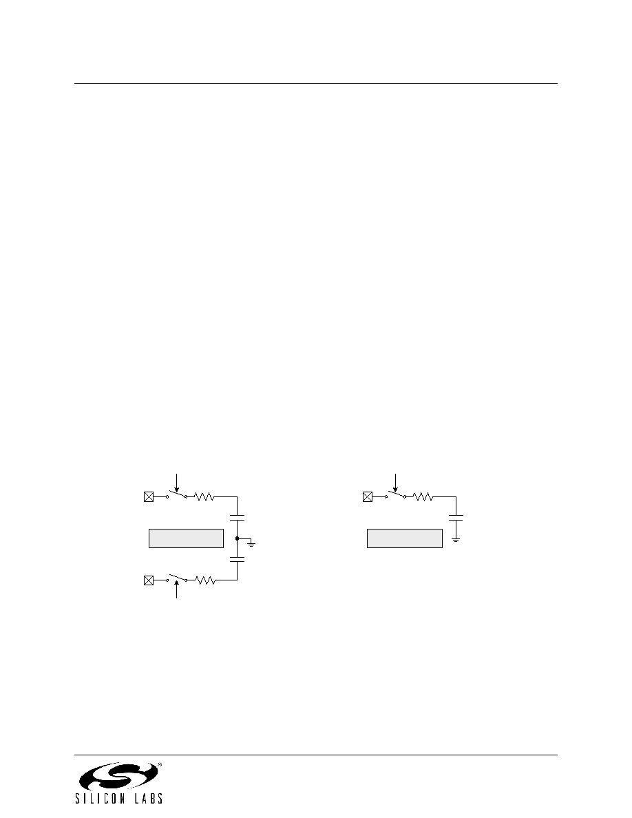
Figure 5.5 shows the equivalent ADC0 input circuits for both Differential and Single-ended modes. Notice
that the equivalent time constant for both input circuits is the same. The required ADC0 settling time for a
given settling accuracy (SA) may be approximated by Equation 5.1. When measuring the Temperature
settling time (track/hold time) requirements.
t
2
n
SA
-------
R
TOTALCSAMPLE
ln
=
Equation 5.1. ADC0 Settling Time Requirements
Where:
SA is the settling accuracy, given as a fraction of an LSB (for example, 0.25 to settle within 1/4 LSB)
t is the required settling time in seconds
RTOTAL is the sum of the AMUX0 resistance and any external source resistance.
n is the ADC resolution in bits (8).
R
MUX = 5k
RC
Input= RMUX * CSAMPLE
R
MUX = 5k
C
SAMPLE = 5pF
C
SAMPLE = 5pF
MUX Select
Differential Mode
P0.x
P0.y
R
MUX = 5k
C
SAMPLE = 5pF
RC
Input= RMUX * CSAMPLE
MUX Select
Single-Ended Mode
P0.x
Note: When the PGA gain is set to 0.5, C
SAMPLE = 3pF
Figure 5.5. ADC0 Equivalent Input Circuits
相关PDF资料 |
PDF描述 |
|---|---|
| AT32UC3C2512C-Z2ZT | IC MCU 32BIT 512KB FLASH 64QFN |
| AU-Y1005-R | CONN USB RTANG FMALE TYPE A PCB |
| USB-B1HSB6 | CONN USB TYPE B R/A BLACK |
| AT32UC3A0256AU-ALUT | IC MCU 256K FLASH 144LQFP |
| AT32UC3C0256C-ALUT | IC MCU AVR32 256K FLASH 144LQFP |
相关代理商/技术参数 |
参数描述 |
|---|---|
| C8051F303-GMR | 功能描述:8位微控制器 -MCU 8KB 11P MCU RoHS:否 制造商:Silicon Labs 核心:8051 处理器系列:C8051F39x 数据总线宽度:8 bit 最大时钟频率:50 MHz 程序存储器大小:16 KB 数据 RAM 大小:1 KB 片上 ADC:Yes 工作电源电压:1.8 V to 3.6 V 工作温度范围:- 40 C to + 105 C 封装 / 箱体:QFN-20 安装风格:SMD/SMT |
| C8051F303-GS | 功能描述:8位微控制器 -MCU 8KB Flash RoHS:否 制造商:Silicon Labs 核心:8051 处理器系列:C8051F39x 数据总线宽度:8 bit 最大时钟频率:50 MHz 程序存储器大小:16 KB 数据 RAM 大小:1 KB 片上 ADC:Yes 工作电源电压:1.8 V to 3.6 V 工作温度范围:- 40 C to + 105 C 封装 / 箱体:QFN-20 安装风格:SMD/SMT |
| C8051F303-GSR | 功能描述:8位微控制器 -MCU 8KB 14Pin MCU RoHS:否 制造商:Silicon Labs 核心:8051 处理器系列:C8051F39x 数据总线宽度:8 bit 最大时钟频率:50 MHz 程序存储器大小:16 KB 数据 RAM 大小:1 KB 片上 ADC:Yes 工作电源电压:1.8 V to 3.6 V 工作温度范围:- 40 C to + 105 C 封装 / 箱体:QFN-20 安装风格:SMD/SMT |
| C8051F303R | 功能描述:8位微控制器 -MCU No ADC RoHS:否 制造商:Silicon Labs 核心:8051 处理器系列:C8051F39x 数据总线宽度:8 bit 最大时钟频率:50 MHz 程序存储器大小:16 KB 数据 RAM 大小:1 KB 片上 ADC:Yes 工作电源电压:1.8 V to 3.6 V 工作温度范围:- 40 C to + 105 C 封装 / 箱体:QFN-20 安装风格:SMD/SMT |
| C8051F304 | 功能描述:8位微控制器 -MCU 4KB RoHS:否 制造商:Silicon Labs 核心:8051 处理器系列:C8051F39x 数据总线宽度:8 bit 最大时钟频率:50 MHz 程序存储器大小:16 KB 数据 RAM 大小:1 KB 片上 ADC:Yes 工作电源电压:1.8 V to 3.6 V 工作温度范围:- 40 C to + 105 C 封装 / 箱体:QFN-20 安装风格:SMD/SMT |
发布紧急采购,3分钟左右您将得到回复。