- 您现在的位置:买卖IC网 > PDF目录17092 > C8051F310-TB (Silicon Laboratories Inc)BOARD PROTOTYPING W/C8051F310 PDF资料下载
参数资料
| 型号: | C8051F310-TB |
| 厂商: | Silicon Laboratories Inc |
| 文件页数: | 208/228页 |
| 文件大小: | 0K |
| 描述: | BOARD PROTOTYPING W/C8051F310 |
| 标准包装: | 1 |
| 类型: | MCU |
| 适用于相关产品: | C8051F310 |
| 所含物品: | 板 |
第1页第2页第3页第4页第5页第6页第7页第8页第9页第10页第11页第12页第13页第14页第15页第16页第17页第18页第19页第20页第21页第22页第23页第24页第25页第26页第27页第28页第29页第30页第31页第32页第33页第34页第35页第36页第37页第38页第39页第40页第41页第42页第43页第44页第45页第46页第47页第48页第49页第50页第51页第52页第53页第54页第55页第56页第57页第58页第59页第60页第61页第62页第63页第64页第65页第66页第67页第68页第69页第70页第71页第72页第73页第74页第75页第76页第77页第78页第79页第80页第81页第82页第83页第84页第85页第86页第87页第88页第89页第90页第91页第92页第93页第94页第95页第96页第97页第98页第99页第100页第101页第102页第103页第104页第105页第106页第107页第108页第109页第110页第111页第112页第113页第114页第115页第116页第117页第118页第119页第120页第121页第122页第123页第124页第125页第126页第127页第128页第129页第130页第131页第132页第133页第134页第135页第136页第137页第138页第139页第140页第141页第142页第143页第144页第145页第146页第147页第148页第149页第150页第151页第152页第153页第154页第155页第156页第157页第158页第159页第160页第161页第162页第163页第164页第165页第166页第167页第168页第169页第170页第171页第172页第173页第174页第175页第176页第177页第178页第179页第180页第181页第182页第183页第184页第185页第186页第187页第188页第189页第190页第191页第192页第193页第194页第195页第196页第197页第198页第199页第200页第201页第202页第203页第204页第205页第206页第207页当前第208页第209页第210页第211页第212页第213页第214页第215页第216页第217页第218页第219页第220页第221页第222页第223页第224页第225页第226页第227页第228页
C8051F310/1/2/3/4/5/6/7
80
Rev. 1.7
Performance
The CIP-51 employs a pipelined architecture that greatly increases its instruction throughput over the stan-
dard 8051 architecture. In a standard 8051, all instructions except for MUL and DIV take 12 or 24 system
clock cycles to execute, and usually have a maximum system clock of 12 MHz. By contrast, the CIP-51
core executes 70% of its instructions in one or two system clock cycles, with no instructions taking more
than eight system clock cycles.
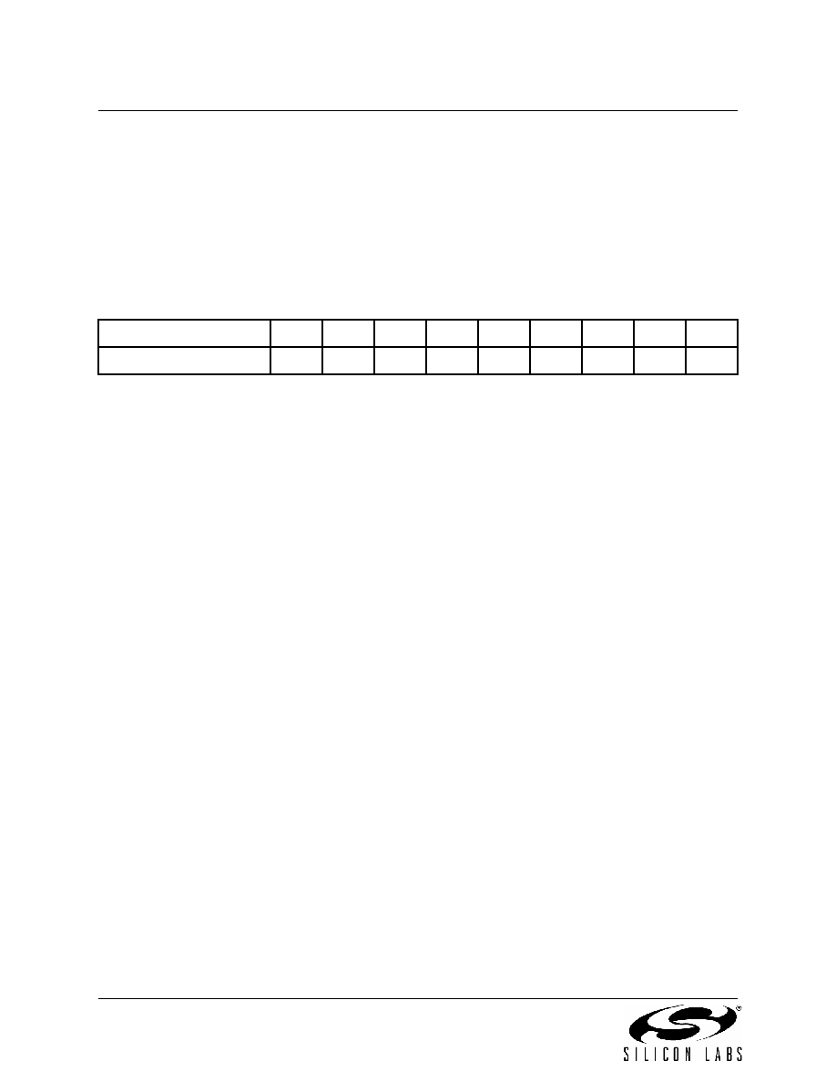
With the CIP-51's maximum system clock at 25 MHz, it has a peak throughput of 25 MIPS. The CIP-51 has
a total of 109 instructions. The table below shows the total number of instructions that require each execu-
tion time.
Clocks to Execute
1
2
2/3
3
3/4
4
4/5
5
8
Number of Instructions
26
50
5
14
7
3
1
2
1
Programming and Debugging Support
In-system programming of the Flash program memory and communication with on-chip debug support
logic is accomplished via the Silicon Labs 2-Wire Development Interface (C2). The re-programmable Flash
can also be read and changed a single byte at a time by the application software using the MOVC and
MOVX instructions. This feature allows program memory to be used for non-volatile data storage as well
as updating program code under software control.
The on-chip debug support logic facilitates full speed in-circuit debugging, allowing the setting of hardware
breakpoints, starting, stopping and single stepping through program execution (including interrupt service
routines), examination of the program's call stack, and reading/writing the contents of registers and mem-
ory. This method of on-chip debugging is completely non-intrusive, requiring no RAM, Stack, timers, or
other on-chip resources. C2 details can be found in Section “20. C2 Interface” on page 223.
The CIP-51 is supported by development tools from Silicon Labs and third party vendors. Silicon Labs pro-
vides an integrated development environment (IDE) including an editor, evaluation compiler, assembler,
debugger and programmer. The IDE's debugger and programmer interface to the CIP-51 via the C2 inter-
face to provide fast and efficient in-system device programming and debugging. Third party macro assem-
blers and C compilers are also available.
8.1.
Instruction Set
The instruction set of the CIP-51 System Controller is fully compatible with the standard MCS-51 instruc-
tion set. Standard 8051 development tools can be used to develop software for the CIP-51. All CIP-51
instructions are the binary and functional equivalent of their MCS-51 counterparts, including opcodes,
addressing modes and effect on PSW flags. However, instruction timing is different than that of the stan-
dard 8051.
8.1.1. Instruction and CPU Timing
In many 8051 implementations, a distinction is made between machine cycles and clock cycles, with
machine cycles varying from 2 to 12 clock cycles in length. However, the CIP-51 implementation is based
solely on clock cycle timing. All instruction timings are specified in terms of clock cycles.
Due to the pipelined architecture of the CIP-51, most instructions execute in the same number of clock
cycles as there are program bytes in the instruction. Conditional branch instructions take one less clock
cycle to complete when the branch is not taken as opposed to when the branch is taken. Table 8.1 is the
相关PDF资料 |
PDF描述 |
|---|---|
| 0210490200 | CABLE JUMPER 1.25MM .152M 14POS |
| LGU2W470MELY | CAP ALUM 47UF 450V 20% SNAP |
| SDR-P | SCOTCH CODE REFILL P |
| 0210490199 | CABLE JUMPER 1.25MM .152M 14POS |
| C8051F411EK | KIT EVAL FOR C8051F411 |
相关代理商/技术参数 |
参数描述 |
|---|---|
| C8051F310-TB-K | 功能描述:BOARD PROTOTYPING W/C8051F310 制造商:silicon labs 系列:- 零件状态:在售 板类型:评估平台 类型:MCU 8-位 核心处理器:8051 操作系统:- 平台:- 配套使用产品/相关产品:C8051F31x 安装类型:固定 内容:板 标准包装:1 |
| C8051F311 | 功能描述:8位微控制器 -MCU 16KB 10ADC RoHS:否 制造商:Silicon Labs 核心:8051 处理器系列:C8051F39x 数据总线宽度:8 bit 最大时钟频率:50 MHz 程序存储器大小:16 KB 数据 RAM 大小:1 KB 片上 ADC:Yes 工作电源电压:1.8 V to 3.6 V 工作温度范围:- 40 C to + 105 C 封装 / 箱体:QFN-20 安装风格:SMD/SMT |
| C8051F311-GM | 功能描述:8位微控制器 -MCU 16KB 10ADC 28P MCU RoHS:否 制造商:Silicon Labs 核心:8051 处理器系列:C8051F39x 数据总线宽度:8 bit 最大时钟频率:50 MHz 程序存储器大小:16 KB 数据 RAM 大小:1 KB 片上 ADC:Yes 工作电源电压:1.8 V to 3.6 V 工作温度范围:- 40 C to + 105 C 封装 / 箱体:QFN-20 安装风格:SMD/SMT |
| C8051F311-GMR | 功能描述:8位微控制器 -MCU 16KB 10ADC 28P MCU RoHS:否 制造商:Silicon Labs 核心:8051 处理器系列:C8051F39x 数据总线宽度:8 bit 最大时钟频率:50 MHz 程序存储器大小:16 KB 数据 RAM 大小:1 KB 片上 ADC:Yes 工作电源电压:1.8 V to 3.6 V 工作温度范围:- 40 C to + 105 C 封装 / 箱体:QFN-20 安装风格:SMD/SMT |
| C8051F311R | 功能描述:8位微控制器 -MCU 10 ADC 28 Pin RoHS:否 制造商:Silicon Labs 核心:8051 处理器系列:C8051F39x 数据总线宽度:8 bit 最大时钟频率:50 MHz 程序存储器大小:16 KB 数据 RAM 大小:1 KB 片上 ADC:Yes 工作电源电压:1.8 V to 3.6 V 工作温度范围:- 40 C to + 105 C 封装 / 箱体:QFN-20 安装风格:SMD/SMT |
发布紧急采购,3分钟左右您将得到回复。