- 您现在的位置:买卖IC网 > PDF目录12011 > C8051F335-GM (Silicon Laboratories Inc)IC 8051 MCU 2KB FLASH 20QFN PDF资料下载
参数资料
| 型号: | C8051F335-GM |
| 厂商: | Silicon Laboratories Inc |
| 文件页数: | 165/210页 |
| 文件大小: | 0K |
| 描述: | IC 8051 MCU 2KB FLASH 20QFN |
| 产品培训模块: | Serial Communication Overview |
| 标准包装: | 91 |
| 系列: | C8051F33x |
| 核心处理器: | 8051 |
| 芯体尺寸: | 8-位 |
| 速度: | 25MHz |
| 连通性: | SMBus(2 线/I²C),SPI,UART/USART |
| 外围设备: | POR,PWM,WDT |
| 输入/输出数: | 17 |
| 程序存储器容量: | 2KB(2K x 8) |
| 程序存储器类型: | 闪存 |
| RAM 容量: | 768 x 8 |
| 电压 - 电源 (Vcc/Vdd): | 2.7 V ~ 3.6 V |
| 振荡器型: | 内部 |
| 工作温度: | -40°C ~ 85°C |
| 封装/外壳: | 20-VFQFN 裸露焊盘 |
| 包装: | 管件 |
| 产品目录页面: | 623 (CN2011-ZH PDF) |
| 配用: | 336-1451-ND - ADAPTER PROGRAM TOOLSTICK F330 |
| 其它名称: | 336-1269 |
第1页第2页第3页第4页第5页第6页第7页第8页第9页第10页第11页第12页第13页第14页第15页第16页第17页第18页第19页第20页第21页第22页第23页第24页第25页第26页第27页第28页第29页第30页第31页第32页第33页第34页第35页第36页第37页第38页第39页第40页第41页第42页第43页第44页第45页第46页第47页第48页第49页第50页第51页第52页第53页第54页第55页第56页第57页第58页第59页第60页第61页第62页第63页第64页第65页第66页第67页第68页第69页第70页第71页第72页第73页第74页第75页第76页第77页第78页第79页第80页第81页第82页第83页第84页第85页第86页第87页第88页第89页第90页第91页第92页第93页第94页第95页第96页第97页第98页第99页第100页第101页第102页第103页第104页第105页第106页第107页第108页第109页第110页第111页第112页第113页第114页第115页第116页第117页第118页第119页第120页第121页第122页第123页第124页第125页第126页第127页第128页第129页第130页第131页第132页第133页第134页第135页第136页第137页第138页第139页第140页第141页第142页第143页第144页第145页第146页第147页第148页第149页第150页第151页第152页第153页第154页第155页第156页第157页第158页第159页第160页第161页第162页第163页第164页当前第165页第166页第167页第168页第169页第170页第171页第172页第173页第174页第175页第176页第177页第178页第179页第180页第181页第182页第183页第184页第185页第186页第187页第188页第189页第190页第191页第192页第193页第194页第195页第196页第197页第198页第199页第200页第201页第202页第203页第204页第205页第206页第207页第208页第209页第210页
Rev. 1.7
61
C8051F330/1/2/3/4/5
7.
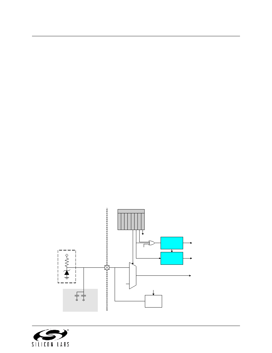
Voltage Reference (C8051F330/2/4 only)
The Voltage reference MUX on the C8051F330/2/4 devices is configurable to use an externally connected
voltage reference, the internal reference voltage generator, or the VDD power supply voltage (see
Figure 7.1). The REFSL bit in the Reference Control register (REF0CN) selects the reference source. For
an external source or the internal reference, REFSL should be set to ‘0’. To use VDD as the reference
source, REFSL should be set to ‘1’.
The BIASE bit enables the internal voltage bias generator, which is used by the ADC, Temperature Sensor,
internal oscillators, and Current DAC. This bias is enabled when any of the aforementioned peripherals are
enabled. The bias generator may be enabled manually by writing a ‘1’ to the BIASE bit in register
REF0CN; see SFR Definition 7.1 for REF0CN register details. The electrical specifications for the voltage
reference circuit are given in Table 7.1.
The internal voltage reference circuit consists of a 1.2 V, temperature stable bandgap voltage reference
generator and a gain-of-two output buffer amplifier. The internal voltage reference can be driven out on the
VREF pin by setting the REFBE bit in register REF0CN to a ‘1’ (see SFR Definition 7.1). The maximum
load seen by the VREF pin must be less than 200 A to GND. When using the internal voltage reference,
bypass capacitors of 0.1 F and 4.7 F are recommended from the VREF pin to GND. If the internal refer-
ence is not used, the REFBE bit should be cleared to ‘0’. Electrical specifications for the internal voltage
reference are given in Table 7.1.
Important Note about the VREF Pin: Port pin P0.0 is used as the external VREF input and as an output
for the internal VREF. When using either an external voltage reference or the internal reference circuitry,
P0.0 should be configured as an analog pin, and skipped by the Digital Crossbar. To configure P0.0 as an
analog pin, set to ‘0’ Bit0 in register P0MDIN. To configure the Crossbar to skip P0.0, set Bit 0 in register
P0SKIP to ‘1’. Refer to Section “14. Port Input/Output” on page 123 for complete Port I/O configuration
details. The TEMPE bit in register REF0CN enables/disables the temperature sensor. While disabled, the
temperature sensor defaults to a high impedance state and any ADC0 measurements performed on the
sensor result in meaningless data.
Figure 7.1. Voltage Reference Functional Block Diagram
VREF
(to ADC)
To Analog Mux
VDD
VREF
R1
VDD
External
Voltage
Reference
Circuit
GND
Temp Sensor
EN
Bias Generator
To ADC, IDAC,
Internal Oscillators
EN
IOSCE
N
0
1
REF0CN
REF
S
L
TEMPE
BI
A
S
E
REF
B
E
REFBE
Internal
Reference
EN
Recommended Bypass
Capacitors
+
4.7
F0.1F
相关PDF资料 |
PDF描述 |
|---|---|
| VI-233-IY-F1 | CONVERTER MOD DC/DC 24V 50W |
| VI-J1T-IY-F2 | CONVERTER MOD DC/DC 6.5V 50W |
| VI-232-IY-F4 | CONVERTER MOD DC/DC 15V 50W |
| VI-232-IY-F3 | CONVERTER MOD DC/DC 15V 50W |
| C8051F520A-IM | IC 8051 MCU 8K FLASH 10DFN |
相关代理商/技术参数 |
参数描述 |
|---|---|
| C8051F335-GMR | 功能描述:8位微控制器 -MCU 2KB 20Pin MCU RoHS:否 制造商:Silicon Labs 核心:8051 处理器系列:C8051F39x 数据总线宽度:8 bit 最大时钟频率:50 MHz 程序存储器大小:16 KB 数据 RAM 大小:1 KB 片上 ADC:Yes 工作电源电压:1.8 V to 3.6 V 工作温度范围:- 40 C to + 105 C 封装 / 箱体:QFN-20 安装风格:SMD/SMT |
| C8051F336 | 制造商:SILABS 制造商全称:SILABS 功能描述:Mixed Signal ISP Flash MCU Family |
| C8051F336DK | 功能描述:开发板和工具包 - 8051 C8051F336 Family Devl Kit RoHS:否 制造商:Silicon Labs 产品:Development Kits 工具用于评估:C8051F960, Si7005 核心: 接口类型:USB 工作电源电压: |
| C8051F336-GM | 功能描述:8位微控制器 -MCU 16KB 10ADC 10DAC 768Ram MCU Lead Free RoHS:否 制造商:Silicon Labs 核心:8051 处理器系列:C8051F39x 数据总线宽度:8 bit 最大时钟频率:50 MHz 程序存储器大小:16 KB 数据 RAM 大小:1 KB 片上 ADC:Yes 工作电源电压:1.8 V to 3.6 V 工作温度范围:- 40 C to + 105 C 封装 / 箱体:QFN-20 安装风格:SMD/SMT |
| C8051F336-GMR | 功能描述:8位微控制器 -MCU 16KB 10ADC 10DAC 768Ram MCU Lead Free RoHS:否 制造商:Silicon Labs 核心:8051 处理器系列:C8051F39x 数据总线宽度:8 bit 最大时钟频率:50 MHz 程序存储器大小:16 KB 数据 RAM 大小:1 KB 片上 ADC:Yes 工作电源电压:1.8 V to 3.6 V 工作温度范围:- 40 C to + 105 C 封装 / 箱体:QFN-20 安装风格:SMD/SMT |
发布紧急采购,3分钟左右您将得到回复。