- 您现在的位置:买卖IC网 > PDF目录11983 > C8051F340-GQ (Silicon Laboratories Inc)IC 8051 MCU FLASH 64K 48TQFP PDF资料下载
参数资料
| 型号: | C8051F340-GQ |
| 厂商: | Silicon Laboratories Inc |
| 文件页数: | 122/276页 |
| 文件大小: | 0K |
| 描述: | IC 8051 MCU FLASH 64K 48TQFP |
| 产品培训模块: | USB Protocol Products USBXpress Serial Communication Overview |
| 标准包装: | 250 |
| 系列: | C8051F34x |
| 核心处理器: | 8051 |
| 芯体尺寸: | 8-位 |
| 速度: | 48MHz |
| 连通性: | EBI/EMI,SMBus(2 线/I²C),SPI,UART/USART,USB |
| 外围设备: | 欠压检测/复位,POR,PWM,温度传感器,WDT |
| 输入/输出数: | 40 |
| 程序存储器容量: | 64KB(64K x 8) |
| 程序存储器类型: | 闪存 |
| RAM 容量: | 4.25K x 8 |
| 电压 - 电源 (Vcc/Vdd): | 2.7 V ~ 3.6 V |
| 数据转换器: | A/D 20x10b |
| 振荡器型: | 内部 |
| 工作温度: | -40°C ~ 85°C |
| 封装/外壳: | 48-TQFP |
| 包装: | 托盘 |
| 配用: | 336-1748-ND - ADAPTER TOOLSTICK FOR C8051F34X 336-1452-ND - ADAPTER PROGRAM TOOLSTICK F340 336-1326-ND - KIT REF DESIGN PWR OVER ETHERNET 336-1307-ND - KIT DEV FOR C8051F34X |
| 其它名称: | 336-1298 |
第1页第2页第3页第4页第5页第6页第7页第8页第9页第10页第11页第12页第13页第14页第15页第16页第17页第18页第19页第20页第21页第22页第23页第24页第25页第26页第27页第28页第29页第30页第31页第32页第33页第34页第35页第36页第37页第38页第39页第40页第41页第42页第43页第44页第45页第46页第47页第48页第49页第50页第51页第52页第53页第54页第55页第56页第57页第58页第59页第60页第61页第62页第63页第64页第65页第66页第67页第68页第69页第70页第71页第72页第73页第74页第75页第76页第77页第78页第79页第80页第81页第82页第83页第84页第85页第86页第87页第88页第89页第90页第91页第92页第93页第94页第95页第96页第97页第98页第99页第100页第101页第102页第103页第104页第105页第106页第107页第108页第109页第110页第111页第112页第113页第114页第115页第116页第117页第118页第119页第120页第121页当前第122页第123页第124页第125页第126页第127页第128页第129页第130页第131页第132页第133页第134页第135页第136页第137页第138页第139页第140页第141页第142页第143页第144页第145页第146页第147页第148页第149页第150页第151页第152页第153页第154页第155页第156页第157页第158页第159页第160页第161页第162页第163页第164页第165页第166页第167页第168页第169页第170页第171页第172页第173页第174页第175页第176页第177页第178页第179页第180页第181页第182页第183页第184页第185页第186页第187页第188页第189页第190页第191页第192页第193页第194页第195页第196页第197页第198页第199页第200页第201页第202页第203页第204页第205页第206页第207页第208页第209页第210页第211页第212页第213页第214页第215页第216页第217页第218页第219页第220页第221页第222页第223页第224页第225页第226页第227页第228页第229页第230页第231页第232页第233页第234页第235页第236页第237页第238页第239页第240页第241页第242页第243页第244页第245页第246页第247页第248页第249页第250页第251页第252页第253页第254页第255页第256页第257页第258页第259页第260页第261页第262页第263页第264页第265页第266页第267页第268页第269页第270页第271页第272页第273页第274页第275页第276页
C8051F340/1/2/3/4/5/6/7/8/9/A/B/C/D
208
Rev. 1.3
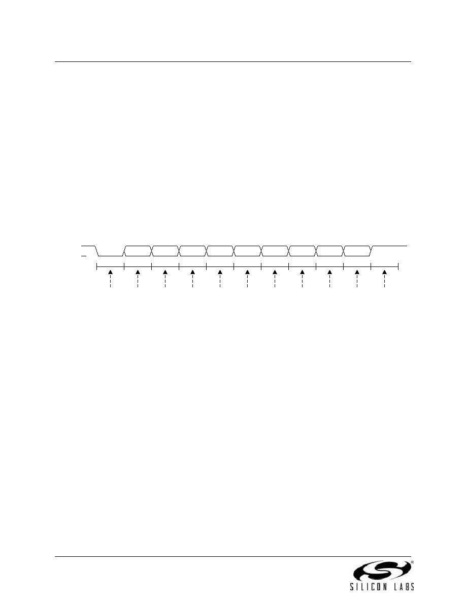
18.2.2. 9-Bit UART
9-bit UART mode uses a total of eleven bits per data byte: a start bit, 8 data bits (LSB first), a programma-
ble ninth data bit, and a stop bit. The state of the ninth transmit data bit is determined by the value in TB80
(SCON0.3), which is assigned by user software. It can be assigned the value of the parity flag (bit P in reg-
ister PSW) for error detection, or used in multiprocessor communications. On receive, the ninth data bit
goes into RB80 (SCON0.2) and the stop bit is ignored.
Data transmission begins when an instruction writes a data byte to the SBUF0 register. The TI0 Transmit
Interrupt Flag (SCON0.1) is set at the end of the transmission (the beginning of the stop-bit time). Data
reception can begin any time after the REN0 Receive Enable bit (SCON0.4) is set to ‘1’. After the stop bit
is received, the data byte will be loaded into the SBUF0 receive register if the following conditions are met:
(1) RI0 must be logic 0, and (2) if MCE0 is logic 1, the 9th bit must be logic 1 (when MCE0 is logic 0, the
state of the ninth data bit is unimportant). If these conditions are met, the eight bits of data are stored in
SBUF0, the ninth bit is stored in RB80, and the RI0 flag is set to ‘1’. If the above conditions are not met,
SBUF0 and RB80 will not be loaded and the RI0 flag will not be set to ‘1’. A UART0 interrupt will occur if
enabled when either TI0 or RI0 is set to ‘1’.
Figure 18.5. 9-Bit UART Timing Diagram
18.3. Multiprocessor Communications
9-Bit UART mode supports multiprocessor communication between a master processor and one or more
slave processors by special use of the ninth data bit. When a master processor wants to transmit to one or
more slaves, it first sends an address byte to select the target(s). An address byte differs from a data byte
in that its ninth bit is logic 1; in a data byte, the ninth bit is always set to logic 0.
Setting the MCE0 bit (SCON0.5) of a slave processor configures its UART such that when a stop bit is
received, the UART will generate an interrupt only if the ninth bit is logic 1 (RB80 = 1) signifying an address
byte has been received. In the UART interrupt handler, software will compare the received address with
the slave's own assigned 8-bit address. If the addresses match, the slave will clear its MCE0 bit to enable
interrupts on the reception of the following data byte(s). Slaves that weren't addressed leave their MCE0
bits set and do not generate interrupts on the reception of the following data bytes, thereby ignoring the
data. Once the entire message is received, the addressed slave resets its MCE0 bit to ignore all transmis-
sions until it receives the next address byte.
Multiple addresses can be assigned to a single slave and/or a single address can be assigned to multiple
slaves, thereby enabling "broadcast" transmissions to more than one slave simultaneously. The master
processor can be configured to receive all transmissions or a protocol can be implemented such that the
master/slave role is temporarily reversed to enable half-duplex transmission between the original master
and slave(s).
D1
D0
D2
D3
D4
D5
D6
D7
START
BIT
MARK
STOP
BIT
BIT TIMES
BIT SAMPLING
SPACE
D8
相关PDF资料 |
PDF描述 |
|---|---|
| P87C51RD2FBD/01,15 | IC 80C51 MCU 8BIT 44LQFP |
| C8051F34A-GQ | IC 8051 MCU 64K FLASH 32LQFP |
| C8051F046-GQ | IC 8051 MCU 32K FLASH 100TQFP |
| C8051F342-GM | IC 8051 MCU 64K FLASH MEM 32-QFN |
| C8051F342-GQ | IC 8051 MCU FLASH 64K 32LQFP |
相关代理商/技术参数 |
参数描述 |
|---|---|
| C8051F340GQR | 制造商:Silicon Laboratories Inc 功能描述:MCU 8-bit C8051F34x 8051 CISC 64KB Flash 3.3V/5V 48-Pin TQFP T/R |
| C8051F340-GQR | 功能描述:8位微控制器 -MCU 48 MIPS 64KB 10ADC RoHS:否 制造商:Silicon Labs 核心:8051 处理器系列:C8051F39x 数据总线宽度:8 bit 最大时钟频率:50 MHz 程序存储器大小:16 KB 数据 RAM 大小:1 KB 片上 ADC:Yes 工作电源电压:1.8 V to 3.6 V 工作温度范围:- 40 C to + 105 C 封装 / 箱体:QFN-20 安装风格:SMD/SMT |
| C8051F340-TB | 功能描述:插座和适配器 PROTO BOARD FOR C8051F340 RoHS:否 制造商:Silicon Labs 产品:Adapter 用于:EM35x |
| C8051F340-TB-K | 功能描述:BOARD PROTOTYPING W/C8051F340 制造商:silicon labs 系列:- 零件状态:在售 板类型:评估平台 类型:MCU 8-位 核心处理器:8051 操作系统:- 平台:- 配套使用产品/相关产品:C8051F340 安装类型:固定 内容:板 标准包装:1 |
| C8051F341 | 制造商:未知厂家 制造商全称:未知厂家 功能描述:Full Speed USB Flash MCU Family |
发布紧急采购,3分钟左右您将得到回复。