- 您现在的位置:买卖IC网 > PDF目录11103 > C8051F343-GM (Silicon Laboratories Inc)IC 8051 MCU 32K FLASH MEM 32-QFN PDF资料下载
参数资料
| 型号: | C8051F343-GM |
| 厂商: | Silicon Laboratories Inc |
| 文件页数: | 96/276页 |
| 文件大小: | 0K |
| 描述: | IC 8051 MCU 32K FLASH MEM 32-QFN |
| 产品培训模块: | Serial Communication Overview |
| 标准包装: | 73 |
| 系列: | C8051F34x |
| 核心处理器: | 8051 |
| 芯体尺寸: | 8-位 |
| 速度: | 48MHz |
| 连通性: | SMBus(2 线/I²C),SPI,UART/USART,USB |
| 外围设备: | 欠压检测/复位,POR,PWM,温度传感器,WDT |
| 输入/输出数: | 25 |
| 程序存储器容量: | 32KB(32K x 8) |
| 程序存储器类型: | 闪存 |
| RAM 容量: | 2.25K x 8 |
| 电压 - 电源 (Vcc/Vdd): | 2.7 V ~ 3.6 V |
| 数据转换器: | A/D 21x10b |
| 振荡器型: | 内部 |
| 工作温度: | -40°C ~ 85°C |
| 封装/外壳: | 32-VFQFN 裸露焊盘 |
| 包装: | 管件 |
| 配用: | 336-1748-ND - ADAPTER TOOLSTICK FOR C8051F34X |
| 其它名称: | 336-1346-5 |
第1页第2页第3页第4页第5页第6页第7页第8页第9页第10页第11页第12页第13页第14页第15页第16页第17页第18页第19页第20页第21页第22页第23页第24页第25页第26页第27页第28页第29页第30页第31页第32页第33页第34页第35页第36页第37页第38页第39页第40页第41页第42页第43页第44页第45页第46页第47页第48页第49页第50页第51页第52页第53页第54页第55页第56页第57页第58页第59页第60页第61页第62页第63页第64页第65页第66页第67页第68页第69页第70页第71页第72页第73页第74页第75页第76页第77页第78页第79页第80页第81页第82页第83页第84页第85页第86页第87页第88页第89页第90页第91页第92页第93页第94页第95页当前第96页第97页第98页第99页第100页第101页第102页第103页第104页第105页第106页第107页第108页第109页第110页第111页第112页第113页第114页第115页第116页第117页第118页第119页第120页第121页第122页第123页第124页第125页第126页第127页第128页第129页第130页第131页第132页第133页第134页第135页第136页第137页第138页第139页第140页第141页第142页第143页第144页第145页第146页第147页第148页第149页第150页第151页第152页第153页第154页第155页第156页第157页第158页第159页第160页第161页第162页第163页第164页第165页第166页第167页第168页第169页第170页第171页第172页第173页第174页第175页第176页第177页第178页第179页第180页第181页第182页第183页第184页第185页第186页第187页第188页第189页第190页第191页第192页第193页第194页第195页第196页第197页第198页第199页第200页第201页第202页第203页第204页第205页第206页第207页第208页第209页第210页第211页第212页第213页第214页第215页第216页第217页第218页第219页第220页第221页第222页第223页第224页第225页第226页第227页第228页第229页第230页第231页第232页第233页第234页第235页第236页第237页第238页第239页第240页第241页第242页第243页第244页第245页第246页第247页第248页第249页第250页第251页第252页第253页第254页第255页第256页第257页第258页第259页第260页第261页第262页第263页第264页第265页第266页第267页第268页第269页第270页第271页第272页第273页第274页第275页第276页
Rev. 1.3
185
C8051F340/1/2/3/4/5/6/7/8/9/A/B/C/D
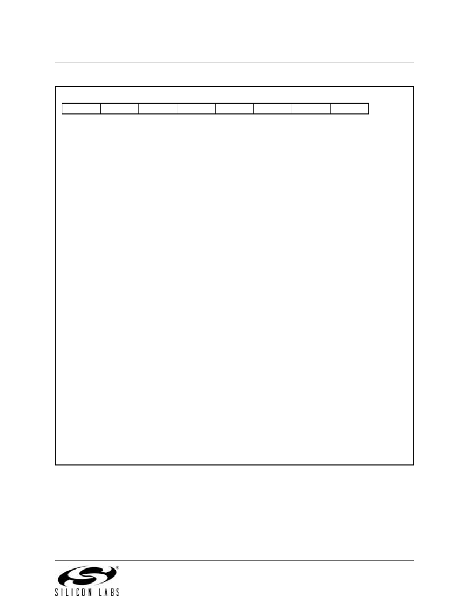
USB Register Definition 16.21. EOUTCSRL: USB0 OUT Endpoint Control Low Byte
Bit7:
CLRDT: Clear Data Toggle
Write:
Software should write ‘1’ to this bit to reset the OUT endpoint data toggle to ‘0’.
Read:
This bit always reads ‘0’.
Bit6:
STSTL: Sent Stall
Hardware sets this bit to ‘1’ when a STALL handshake signal is transmitted. This flag must
be cleared by software.
Bit5:
SDSTL: Send Stall
Software should write ‘1’ to this bit to generate a STALL handshake. Software should write
‘0’ to this bit to terminate the STALL signal. This bit has no effect in ISO mode.
Bit4:
FLUSH: FIFO Flush
Writing a ‘1’ to this bit flushes the next packet to be read from the OUT endpoint FIFO. The
FIFO pointer is reset and the OPRDY bit is cleared. If the FIFO contains multiple packets,
software must write ‘1’ to FLUSH for each packet. Hardware resets the FLUSH bit to ‘0’
when the FIFO flush is complete.
Note: If data for the current packet has already been read from the FIFO, the FLUSH bit should
not be used to flush the packet. Instead, the entire data packet should be read from the
FIFO manually.
Bit3:
DATERR: Data Error
In ISO mode, this bit is set by hardware if a received packet has a CRC or bit-stuffing error.
It is cleared when software clears OPRDY. This bit is only valid in ISO mode.
Bit2:
OVRUN: Data Overrun
This bit is set by hardware when an incoming data packet cannot be loaded into the OUT
endpoint FIFO. This bit is only valid in ISO mode, and must be cleared by software.
0: No data overrun.
1: A data packet was lost because of a full FIFO since this flag was last cleared.
Bit1:
FIFOFUL: OUT FIFO Full
This bit indicates the contents of the OUT FIFO. If double buffering is enabled for the end-
point (DBIEN = ‘1’), the FIFO is full when the FIFO contains two packets. If DBIEN = ‘0’, the
FIFO is full when the FIFO contains one packet.
0: OUT endpoint FIFO is not full.
1: OUT endpoint FIFO is full.
Bit0:
OPRDY: OUT Packet Ready
Hardware sets this bit to ‘1’ and generates an interrupt when a data packet is available. Soft-
ware should clear this bit after each data packet is unloaded from the OUT endpoint FIFO.
W
R/W
R
R/W
R
R/W
Reset Value
CLRDT
STSTL
SDSTL
FLUSH
DATERR
OVRUN
FIFOFUL
OPRDY
00000000
Bit7
Bit6
Bit5
Bit4
Bit3
Bit2
Bit1
Bit0
USB Address:
0x14
相关PDF资料 |
PDF描述 |
|---|---|
| VE-B7X-IY-F3 | CONVERTER MOD DC/DC 5.2V 50W |
| VE-24M-IW | CONVERTER MOD DC/DC 10V 100W |
| VE-B7X-IY-F2 | CONVERTER MOD DC/DC 5.2V 50W |
| VE-B7W-IY-F4 | CONVERTER MOD DC/DC 5.5V 50W |
| VE-B7W-IY-F3 | CONVERTER MOD DC/DC 5.5V 50W |
相关代理商/技术参数 |
参数描述 |
|---|---|
| C8051F343-GMR | 功能描述:8位微控制器 -MCU 48 MIPS 32KB 10 ADC RoHS:否 制造商:Silicon Labs 核心:8051 处理器系列:C8051F39x 数据总线宽度:8 bit 最大时钟频率:50 MHz 程序存储器大小:16 KB 数据 RAM 大小:1 KB 片上 ADC:Yes 工作电源电压:1.8 V to 3.6 V 工作温度范围:- 40 C to + 105 C 封装 / 箱体:QFN-20 安装风格:SMD/SMT |
| C8051F343-GQ | 功能描述:8位微控制器 -MCU 48 MIPS 32KB 10ADC RoHS:否 制造商:Silicon Labs 核心:8051 处理器系列:C8051F39x 数据总线宽度:8 bit 最大时钟频率:50 MHz 程序存储器大小:16 KB 数据 RAM 大小:1 KB 片上 ADC:Yes 工作电源电压:1.8 V to 3.6 V 工作温度范围:- 40 C to + 105 C 封装 / 箱体:QFN-20 安装风格:SMD/SMT |
| C8051F343-GQR | 功能描述:8位微控制器 -MCU 48 MIPS 32KB 10ADC RoHS:否 制造商:Silicon Labs 核心:8051 处理器系列:C8051F39x 数据总线宽度:8 bit 最大时钟频率:50 MHz 程序存储器大小:16 KB 数据 RAM 大小:1 KB 片上 ADC:Yes 工作电源电压:1.8 V to 3.6 V 工作温度范围:- 40 C to + 105 C 封装 / 箱体:QFN-20 安装风格:SMD/SMT |
| C8051F344 | 制造商:SILABS 制造商全称:SILABS 功能描述:Full Speed USB Flash MCU Family |
| C8051F344-GQ | 功能描述:8位微控制器 -MCU 25 MIPS 64KB 10ADC RoHS:否 制造商:Silicon Labs 核心:8051 处理器系列:C8051F39x 数据总线宽度:8 bit 最大时钟频率:50 MHz 程序存储器大小:16 KB 数据 RAM 大小:1 KB 片上 ADC:Yes 工作电源电压:1.8 V to 3.6 V 工作温度范围:- 40 C to + 105 C 封装 / 箱体:QFN-20 安装风格:SMD/SMT |
发布紧急采购,3分钟左右您将得到回复。