- 您现在的位置:买卖IC网 > PDF目录3794 > C8051F411-GM (Silicon Laboratories Inc)IC 8051 MCU 32K FLASH 28QFN PDF资料下载
参数资料
| 型号: | C8051F411-GM |
| 厂商: | Silicon Laboratories Inc |
| 文件页数: | 105/270页 |
| 文件大小: | 0K |
| 描述: | IC 8051 MCU 32K FLASH 28QFN |
| 产品培训模块: | Serial Communication Overview |
| 标准包装: | 73 |
| 系列: | C8051F41x |
| 核心处理器: | 8051 |
| 芯体尺寸: | 8-位 |
| 速度: | 50MHz |
| 连通性: | SMBus(2 线/I²C),SPI,UART/USART |
| 外围设备: | 欠压检测/复位,POR,PWM,温度传感器,WDT |
| 输入/输出数: | 20 |
| 程序存储器容量: | 32KB(32K x 8) |
| 程序存储器类型: | 闪存 |
| RAM 容量: | 2.25K x 8 |
| 电压 - 电源 (Vcc/Vdd): | 2 V ~ 5.25 V |
| 数据转换器: | A/D 20x12b; D/A 2x12b |
| 振荡器型: | 内部 |
| 工作温度: | -40°C ~ 85°C |
| 封装/外壳: | 28-VFQFN 裸露焊盘 |
| 包装: | 管件 |
| 配用: | 336-1454-ND - ADAPTER PROGRAM TOOLSTICK F411 336-1317-ND - KIT EVAL FOR C8051F411 336-1314-ND - KIT DEV FOR C8051F41X |
| 其它名称: | 336-1309 |
第1页第2页第3页第4页第5页第6页第7页第8页第9页第10页第11页第12页第13页第14页第15页第16页第17页第18页第19页第20页第21页第22页第23页第24页第25页第26页第27页第28页第29页第30页第31页第32页第33页第34页第35页第36页第37页第38页第39页第40页第41页第42页第43页第44页第45页第46页第47页第48页第49页第50页第51页第52页第53页第54页第55页第56页第57页第58页第59页第60页第61页第62页第63页第64页第65页第66页第67页第68页第69页第70页第71页第72页第73页第74页第75页第76页第77页第78页第79页第80页第81页第82页第83页第84页第85页第86页第87页第88页第89页第90页第91页第92页第93页第94页第95页第96页第97页第98页第99页第100页第101页第102页第103页第104页当前第105页第106页第107页第108页第109页第110页第111页第112页第113页第114页第115页第116页第117页第118页第119页第120页第121页第122页第123页第124页第125页第126页第127页第128页第129页第130页第131页第132页第133页第134页第135页第136页第137页第138页第139页第140页第141页第142页第143页第144页第145页第146页第147页第148页第149页第150页第151页第152页第153页第154页第155页第156页第157页第158页第159页第160页第161页第162页第163页第164页第165页第166页第167页第168页第169页第170页第171页第172页第173页第174页第175页第176页第177页第178页第179页第180页第181页第182页第183页第184页第185页第186页第187页第188页第189页第190页第191页第192页第193页第194页第195页第196页第197页第198页第199页第200页第201页第202页第203页第204页第205页第206页第207页第208页第209页第210页第211页第212页第213页第214页第215页第216页第217页第218页第219页第220页第221页第222页第223页第224页第225页第226页第227页第228页第229页第230页第231页第232页第233页第234页第235页第236页第237页第238页第239页第240页第241页第242页第243页第244页第245页第246页第247页第248页第249页第250页第251页第252页第253页第254页第255页第256页第257页第258页第259页第260页第261页第262页第263页第264页第265页第266页第267页第268页第269页第270页
Rev. 1.1
193
C8051F410/1/2/3
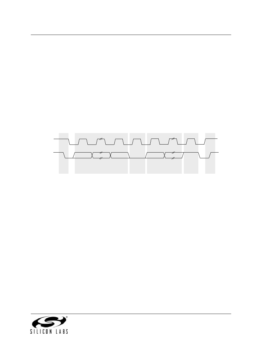
A typical SMBus transaction consists of a START condition followed by an address byte (Bits7-1: 7-bit
slave address; Bit0: R/W direction bit), one or more bytes of data, and a STOP condition. Each byte that is
received (by a master or slave) must be acknowledged (ACK) with a low SDA during a high SCL (see
Figure 21.3). If the receiving device does not ACK, the transmitting device will read a NACK (not acknowl-
edge), which is a high SDA during a high SCL.
The direction bit (R/W) occupies the least-significant bit position of the address byte. The direction bit is set
to logic 1 to indicate a "READ" operation and cleared to logic 0 to indicate a "WRITE" operation.
All transactions are initiated by a master, with one or more addressed slave devices as the target.
The
master generates the START condition and then transmits the slave address and direction bit. If the trans-
action is a WRITE operation from the master to the slave, the master transmits the data a byte at a time
waiting for an ACK from the slave at the end of each byte. For READ operations, the slave transmits the
data waiting for an ACK from the master at the end of each byte. At the end of the data transfer, the master
generates a STOP condition to terminate the transaction and free the bus. Figure 21.3 illustrates a typical
SMBus transaction.
SLA6
SDA
SLA5-0
R/W
D7
D6-0
SCL
Slave Address + R/W
Data Byte
START
ACK
NACK
STOP
Figure 21.3. SMBus Transaction
21.3.1. Arbitration
A master may start a transfer only if the bus is free. The bus is free after a STOP condition or after the SCL
and SDA lines remain high for a specified time (see
on page 194). In the event that two or more devices attempt to begin a transfer at the same time, an arbi-
tration scheme is employed to force one master to give up the bus. The master devices continue transmit-
ting until one attempts a HIGH while the other transmits a LOW. Since the bus is open-drain, the bus will
be pulled LOW. The master attempting the HIGH will detect a LOW SDA and lose the arbitration. The win-
ning master continues its transmission without interruption; the losing master becomes a slave and
receives the rest of the transfer if addressed. This arbitration scheme is non-destructive: one device
always wins, and no data is lost.
21.3.2. Clock Low Extension
SMBus provides a clock synchronization mechanism, similar to I2C, which allows devices with different
speed capabilities to coexist on the bus. A clock-low extension is used during a transfer in order to allow
slower slave devices to communicate with faster masters. The slave may temporarily hold the SCL line
LOW to extend the clock low period, effectively decreasing the serial clock frequency.
相关PDF资料 |
PDF描述 |
|---|---|
| MC68331CFC16B1 | IC MCU 32BIT 16MHZ 132-PQFP |
| MC68331CFC16 | IC MCU 32BIT 16MHZ 132-PQFP |
| C8051F587-IM | IC 8051 MCU 96K FLASH 32-QFN |
| LPC11U24FBD48/401, | IC MCU USB 48LQFP |
| LPC11U24FHN33/401, | MCU USB 33HVQFN |
相关代理商/技术参数 |
参数描述 |
|---|---|
| C8051F411-GMR | 功能描述:8位微控制器 -MCU 50 MIPS 32KB 12ADC RTCLOCK 28 PIN MCU RoHS:否 制造商:Silicon Labs 核心:8051 处理器系列:C8051F39x 数据总线宽度:8 bit 最大时钟频率:50 MHz 程序存储器大小:16 KB 数据 RAM 大小:1 KB 片上 ADC:Yes 工作电源电压:1.8 V to 3.6 V 工作温度范围:- 40 C to + 105 C 封装 / 箱体:QFN-20 安装风格:SMD/SMT |
| C8051F412 | 制造商:SILABS 制造商全称:SILABS 功能描述:2.0 V, 32/16 kB Flash, smaRTClock, 12-bit ADC |
| C8051F412-GQ | 功能描述:8位微控制器 -MCU 50 MIPS 16KB 12ADC RTCLOCK 32 PIN MCU RoHS:否 制造商:Silicon Labs 核心:8051 处理器系列:C8051F39x 数据总线宽度:8 bit 最大时钟频率:50 MHz 程序存储器大小:16 KB 数据 RAM 大小:1 KB 片上 ADC:Yes 工作电源电压:1.8 V to 3.6 V 工作温度范围:- 40 C to + 105 C 封装 / 箱体:QFN-20 安装风格:SMD/SMT |
| C8051F412-GQR | 功能描述:8位微控制器 -MCU 50 MIPS 16KB 12ADC RTCLOCK 32 PIN MCU RoHS:否 制造商:Silicon Labs 核心:8051 处理器系列:C8051F39x 数据总线宽度:8 bit 最大时钟频率:50 MHz 程序存储器大小:16 KB 数据 RAM 大小:1 KB 片上 ADC:Yes 工作电源电压:1.8 V to 3.6 V 工作温度范围:- 40 C to + 105 C 封装 / 箱体:QFN-20 安装风格:SMD/SMT |
| C8051F413 | 制造商:SILABS 制造商全称:SILABS 功能描述:2.0 V, 32/16 kB Flash, smaRTClock, 12-bit ADC |
发布紧急采购,3分钟左右您将得到回复。