- 您现在的位置:买卖IC网 > PDF目录12012 > C8051F520-IM (Silicon Laboratories Inc)IC 8051 MCU 8K FLASH 10DFN PDF资料下载
参数资料
| 型号: | C8051F520-IM |
| 厂商: | Silicon Laboratories Inc |
| 文件页数: | 172/220页 |
| 文件大小: | 0K |
| 描述: | IC 8051 MCU 8K FLASH 10DFN |
| 标准包装: | 122 |
| 系列: | C8051F52x |
| 核心处理器: | 8051 |
| 芯体尺寸: | 8-位 |
| 速度: | 25MHz |
| 连通性: | LIN,SPI,UART/USART |
| 外围设备: | 欠压检测/复位,POR,PWM,温度传感器,WDT |
| 输入/输出数: | 6 |
| 程序存储器容量: | 8KB(8K x 8) |
| 程序存储器类型: | 闪存 |
| RAM 容量: | 256 x 8 |
| 电压 - 电源 (Vcc/Vdd): | 2 V ~ 5.25 V |
| 数据转换器: | A/D 6x12b |
| 振荡器型: | 内部 |
| 工作温度: | -40°C ~ 125°C |
| 封装/外壳: | 10-VFDFN 裸露焊盘 |
| 包装: | 管件 |
| 其它名称: | 336-1341 |
第1页第2页第3页第4页第5页第6页第7页第8页第9页第10页第11页第12页第13页第14页第15页第16页第17页第18页第19页第20页第21页第22页第23页第24页第25页第26页第27页第28页第29页第30页第31页第32页第33页第34页第35页第36页第37页第38页第39页第40页第41页第42页第43页第44页第45页第46页第47页第48页第49页第50页第51页第52页第53页第54页第55页第56页第57页第58页第59页第60页第61页第62页第63页第64页第65页第66页第67页第68页第69页第70页第71页第72页第73页第74页第75页第76页第77页第78页第79页第80页第81页第82页第83页第84页第85页第86页第87页第88页第89页第90页第91页第92页第93页第94页第95页第96页第97页第98页第99页第100页第101页第102页第103页第104页第105页第106页第107页第108页第109页第110页第111页第112页第113页第114页第115页第116页第117页第118页第119页第120页第121页第122页第123页第124页第125页第126页第127页第128页第129页第130页第131页第132页第133页第134页第135页第136页第137页第138页第139页第140页第141页第142页第143页第144页第145页第146页第147页第148页第149页第150页第151页第152页第153页第154页第155页第156页第157页第158页第159页第160页第161页第162页第163页第164页第165页第166页第167页第168页第169页第170页第171页当前第172页第173页第174页第175页第176页第177页第178页第179页第180页第181页第182页第183页第184页第185页第186页第187页第188页第189页第190页第191页第192页第193页第194页第195页第196页第197页第198页第199页第200页第201页第202页第203页第204页第205页第206页第207页第208页第209页第210页第211页第212页第213页第214页第215页第216页第217页第218页第219页第220页
Rev. 1.4
55
C8051F52x/F53x
Post-Tracking Mode is selected when AD0TM is set to 01b. A programmable tracking time based on
AD0TK is started immediately following the convert start signal. Conversions are started after the pro-
grammed tracking time ends. After a conversion is complete, ADC0 does not track the input. Rather, the
sampling capacitor remains disconnected from the input making the input pin high-impedance until the
next convert start signal.
Dual-Tracking Mode is selected when AD0TM is set to 11b. A programmable tracking time based on
AD0TK is started immediately following the convert start signal. Conversions are started after the pro-
grammed tracking time ends. After a conversion is complete, ADC0 tracks continuously until the next con-
version is started.
Depending on the output connected to the ADC input, additional tracking time, more than is specified in
Table 2.3 on page 28, may be required after changing MUX settings. See the settling time requirements
Figure 4.3. ADC0 Tracking Modes
4.3.3. Timing
ADC0 has a maximum conversion speed specified in Table 2.3 on page 28. ADC0 is clocked from the
ADC0 Subsystem Clock (FCLK). The source of FCLK is selected based on the BURSTEN bit. When
BURSTEN is logic 0, FCLK is derived from the current system clock. When BURSTEN is logic 1, FCLK is
derived from the Burst Mode Oscillator, which is an independent clock source whose maximum frequency
is specified in Table 2.3 on page 28.
When ADC0 is performing a conversion, it requires a clock source that is typically slower than FCLK. The
ADC0 SAR conversion clock (SAR clock) is a divided version of FCLK. The divide ratio can be configured
using the AD0SC bits in the ADC0CF register. The maximum SAR clock frequency is listed in Table 2.3 on
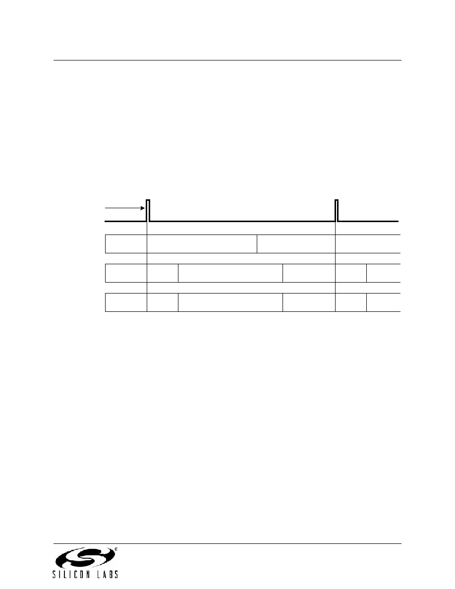
ADC0 can be in one of three states at any given time: tracking, converting, or idle. Tracking time depends
on the tracking mode selected. For Pre-Tracking Mode, tracking is managed by software and ADC0 starts
conversions immediately following the convert start signal. For Post-Tracking and Dual-Tracking Modes,
the tracking time after the convert start signal is equal to the value determined by the AD0TK bits plus 2
FCLK cycles. Tracking is immediately followed by a conversion. The ADC0 conversion time is always 13
SAR clock cycles plus an additional 2 FCLK cycles to start and complete a conversion. Figure 4.4 shows
timing diagrams for a conversion in Pre-Tracking Mode and tracking plus conversion in Post-Tracking or
Dual-Tracking Mode. In this example, repeat count is set to one.
Convert Start
Post-Tracking
AD0TM= 01
Track
Convert
Idle
Track
Convert..
Pre-Tracking
AD0TM = 10
Track
Convert
Track
Convert ...
Dual-Tracking
AD0TM = 11
Track
Convert
Track
Convert..
相关PDF资料 |
PDF描述 |
|---|---|
| VE-JWL-IY-F3 | CONVERTER MOD DC/DC 28V 50W |
| VE-JWK-IY-F4 | CONVERTER MOD DC/DC 40V 50W |
| VE-JWJ-IY-F3 | CONVERTER MOD DC/DC 36V 50W |
| VE-JWH-IY-F1 | CONVERTER MOD DC/DC 52V 50W |
| C8051F988-GM | IC MCU 8BIT 4KB FLASH 24QFN |
相关代理商/技术参数 |
参数描述 |
|---|---|
| C8051F520-IMR | 功能描述:8位微控制器 -MCU 8KB 12ADC 125C RoHS:否 制造商:Silicon Labs 核心:8051 处理器系列:C8051F39x 数据总线宽度:8 bit 最大时钟频率:50 MHz 程序存储器大小:16 KB 数据 RAM 大小:1 KB 片上 ADC:Yes 工作电源电压:1.8 V to 3.6 V 工作温度范围:- 40 C to + 105 C 封装 / 箱体:QFN-20 安装风格:SMD/SMT |
| C8051F521A-IM | 功能描述:8位微控制器 -MCU 8KB 12ADC 125C MCU RoHS:否 制造商:Silicon Labs 核心:8051 处理器系列:C8051F39x 数据总线宽度:8 bit 最大时钟频率:50 MHz 程序存储器大小:16 KB 数据 RAM 大小:1 KB 片上 ADC:Yes 工作电源电压:1.8 V to 3.6 V 工作温度范围:- 40 C to + 105 C 封装 / 箱体:QFN-20 安装风格:SMD/SMT |
| C8051F521A-IMR | 功能描述:8位微控制器 -MCU 25 MIPS 8 kB 256 SPI RoHS:否 制造商:Silicon Labs 核心:8051 处理器系列:C8051F39x 数据总线宽度:8 bit 最大时钟频率:50 MHz 程序存储器大小:16 KB 数据 RAM 大小:1 KB 片上 ADC:Yes 工作电源电压:1.8 V to 3.6 V 工作温度范围:- 40 C to + 105 C 封装 / 箱体:QFN-20 安装风格:SMD/SMT |
| C8051F521-C-IM | 制造商:Silicon Laboratories Inc 功能描述:25 MIPS, 8 KB, 256, SPI, UART, DFN10 - Rail/Tube 制造商:Silicon Laboratories Inc 功能描述:IC MCU 8051 8KB FLASH 10DFN |
| C8051F521-C-IMR | 制造商:Silicon Laboratories Inc 功能描述:25 MIPS, 8 KB, 256, SPI, UART, DFN10 - Tape and Reel 制造商:Silicon Laboratories Inc 功能描述:IC MCU 8051 8KB FLASH 10DFN |
发布紧急采购,3分钟左右您将得到回复。