- 您现在的位置:买卖IC网 > PDF目录11171 > C8051F801-GM (Silicon Laboratories Inc)IC MCU 8BIT 16KB FLASH 20QFN PDF资料下载
参数资料
| 型号: | C8051F801-GM |
| 厂商: | Silicon Laboratories Inc |
| 文件页数: | 126/250页 |
| 文件大小: | 0K |
| 描述: | IC MCU 8BIT 16KB FLASH 20QFN |
| 产品培训模块: | Serial Communication Overview |
| 特色产品: | QuickSense? Portfolio |
| 标准包装: | 91 |
| 系列: | C8051F80x |
| 核心处理器: | 8051 |
| 芯体尺寸: | 8-位 |
| 速度: | 25MHz |
| 连通性: | SMBus(2 线/I²C),SPI,UART/USART |
| 外围设备: | 电容感应,POR,PWM,温度传感器,WDT |
| 输入/输出数: | 17 |
| 程序存储器容量: | 16KB(16K x 8) |
| 程序存储器类型: | 闪存 |
| RAM 容量: | 512 x 8 |
| 电压 - 电源 (Vcc/Vdd): | 1.8 V ~ 3.6 V |
| 数据转换器: | A/D 16x10b |
| 振荡器型: | 内部 |
| 工作温度: | -40°C ~ 85°C |
| 封装/外壳: | 20-VFQFN 裸露焊盘 |
| 包装: | 管件 |
| 产品目录页面: | 624 (CN2011-ZH PDF) |
| 其它名称: | 336-1768-5 |
第1页第2页第3页第4页第5页第6页第7页第8页第9页第10页第11页第12页第13页第14页第15页第16页第17页第18页第19页第20页第21页第22页第23页第24页第25页第26页第27页第28页第29页第30页第31页第32页第33页第34页第35页第36页第37页第38页第39页第40页第41页第42页第43页第44页第45页第46页第47页第48页第49页第50页第51页第52页第53页第54页第55页第56页第57页第58页第59页第60页第61页第62页第63页第64页第65页第66页第67页第68页第69页第70页第71页第72页第73页第74页第75页第76页第77页第78页第79页第80页第81页第82页第83页第84页第85页第86页第87页第88页第89页第90页第91页第92页第93页第94页第95页第96页第97页第98页第99页第100页第101页第102页第103页第104页第105页第106页第107页第108页第109页第110页第111页第112页第113页第114页第115页第116页第117页第118页第119页第120页第121页第122页第123页第124页第125页当前第126页第127页第128页第129页第130页第131页第132页第133页第134页第135页第136页第137页第138页第139页第140页第141页第142页第143页第144页第145页第146页第147页第148页第149页第150页第151页第152页第153页第154页第155页第156页第157页第158页第159页第160页第161页第162页第163页第164页第165页第166页第167页第168页第169页第170页第171页第172页第173页第174页第175页第176页第177页第178页第179页第180页第181页第182页第183页第184页第185页第186页第187页第188页第189页第190页第191页第192页第193页第194页第195页第196页第197页第198页第199页第200页第201页第202页第203页第204页第205页第206页第207页第208页第209页第210页第211页第212页第213页第214页第215页第216页第217页第218页第219页第220页第221页第222页第223页第224页第225页第226页第227页第228页第229页第230页第231页第232页第233页第234页第235页第236页第237页第238页第239页第240页第241页第242页第243页第244页第245页第246页第247页第248页第249页第250页
Rev. 1.0
211
C8051F80x-83x
28.1. Timer 0 and Timer 1
Each timer is implemented as a 16-bit register accessed as two separate bytes: a low byte (TL0 or TL1)
and a high byte (TH0 or TH1). The Counter/Timer Control register (TCON) is used to enable Timer 0 and
Timer 1 as well as indicate status. Timer 0 interrupts can be enabled by setting the ET0 bit in the IE regis-
ter (Section “18.2. Interrupt Register Descriptions” on page 104); Timer 1 interrupts can be enabled by set-
ting the ET1 bit in the IE register (Section “18.2. Interrupt Register Descriptions” on page 104). Both
counter/timers operate in one of four primary modes selected by setting the Mode Select bits T1M1–T0M0
in the Counter/Timer Mode register (TMOD). Each timer can be configured independently. Each operating
mode is described below.
28.1.1. Mode 0: 13-bit Counter/Timer
Timer 0 and Timer 1 operate as 13-bit counter/timers in Mode 0. The following describes the configuration
and operation of Timer 0. However, both timers operate identically, and Timer 1 is configured in the same
manner as described for Timer 0.
The TH0 register holds the eight MSBs of the 13-bit counter/timer. TL0 holds the five LSBs in bit positions
TL0.4–TL0.0. The three upper bits of TL0 (TL0.7–TL0.5) are indeterminate and should be masked out or
ignored when reading. As the 13-bit timer register increments and overflows from 0x1FFF (all ones) to
0x0000, the timer overflow flag TF0 in TCON is set and an interrupt will occur if Timer 0 interrupts are
enabled.
The C/T0 bit in the TMOD register selects the counter/timer's clock source. When C/T0 is set to logic 1,
high-to-low transitions at the selected Timer 0 input pin (T0) increment the timer register (Refer to Section
“23.3. Priority Crossbar Decoder” on page 143 for information on selecting and configuring external I/O
pins). Clearing C/T selects the clock defined by the T0M bit in register CKCON. When T0M is set, Timer 0
is clocked by the system clock. When T0M is cleared, Timer 0 is clocked by the source selected by the
Clock Scale bits in CKCON (see SFR Definition 28.1).
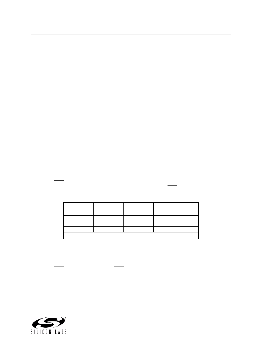
Setting the TR0 bit (TCON.4) enables the timer when either GATE0 in the TMOD register is logic 0 or the
input signal INT0 is active as defined by bit IN0PL in register IT01CF (see SFR Definition 18.7). Setting
GATE0 to 1 allows the timer to be controlled by the external input signal INT0 (see Section “18.2. Interrupt
Register Descriptions” on page 104), facilitating pulse width measurements
Setting TR0 does not force the timer to reset. The timer registers should be loaded with the desired initial
value before the timer is enabled.
TL1 and TH1 form the 13-bit register for Timer 1 in the same manner as described above for TL0 and TH0.
Timer 1 is configured and controlled using the relevant TCON and TMOD bits just as with Timer 0. The
input signal INT1 is used with Timer 1; the INT1 polarity is defined by bit IN1PL in register IT01CF (see
TR0
GATE0
INT0
Counter/Timer
0
X
Disabled
1
0
X
Enabled
1
0
Disabled
1
Enabled
Note:
X = Don't Care
相关PDF资料 |
PDF描述 |
|---|---|
| ISL84684IR | IC SWITCH DUAL SPDT 10TDFN |
| C8051F804-GS | IC MCU 8BIT 16KB FLASH 16SOIC |
| HI9P0508-5Z96 | IC MULTIPLEXER 8X1 16SOIC |
| ISL8325IBZ | IC SWITCH DUAL SPST 8SOIC |
| ISL8324IBZ | IC SWITCH DUAL SPST 8SOIC |
相关代理商/技术参数 |
参数描述 |
|---|---|
| C8051F801-GMR | 功能描述:8位微控制器 -MCU 16kB 512B RAM ADC 8-CH CDC RoHS:否 制造商:Silicon Labs 核心:8051 处理器系列:C8051F39x 数据总线宽度:8 bit 最大时钟频率:50 MHz 程序存储器大小:16 KB 数据 RAM 大小:1 KB 片上 ADC:Yes 工作电源电压:1.8 V to 3.6 V 工作温度范围:- 40 C to + 105 C 封装 / 箱体:QFN-20 安装风格:SMD/SMT |
| C8051F801-GU | 功能描述:8位微控制器 -MCU 16kB, 512B RAM, ADC, 8-ch CDC RoHS:否 制造商:Silicon Labs 核心:8051 处理器系列:C8051F39x 数据总线宽度:8 bit 最大时钟频率:50 MHz 程序存储器大小:16 KB 数据 RAM 大小:1 KB 片上 ADC:Yes 工作电源电压:1.8 V to 3.6 V 工作温度范围:- 40 C to + 105 C 封装 / 箱体:QFN-20 安装风格:SMD/SMT |
| C8051F801-GUR | 功能描述:8位微控制器 -MCU 16kB 512B RAM ADC 8-CH CDC RoHS:否 制造商:Silicon Labs 核心:8051 处理器系列:C8051F39x 数据总线宽度:8 bit 最大时钟频率:50 MHz 程序存储器大小:16 KB 数据 RAM 大小:1 KB 片上 ADC:Yes 工作电源电压:1.8 V to 3.6 V 工作温度范围:- 40 C to + 105 C 封装 / 箱体:QFN-20 安装风格:SMD/SMT |
| C8051F802-GM | 功能描述:8位微控制器 -MCU 16kB, 512B RAM, ADC RoHS:否 制造商:Silicon Labs 核心:8051 处理器系列:C8051F39x 数据总线宽度:8 bit 最大时钟频率:50 MHz 程序存储器大小:16 KB 数据 RAM 大小:1 KB 片上 ADC:Yes 工作电源电压:1.8 V to 3.6 V 工作温度范围:- 40 C to + 105 C 封装 / 箱体:QFN-20 安装风格:SMD/SMT |
| C8051F802-GMR | 功能描述:8位微控制器 -MCU 16kB 512B RAM ADC RoHS:否 制造商:Silicon Labs 核心:8051 处理器系列:C8051F39x 数据总线宽度:8 bit 最大时钟频率:50 MHz 程序存储器大小:16 KB 数据 RAM 大小:1 KB 片上 ADC:Yes 工作电源电压:1.8 V to 3.6 V 工作温度范围:- 40 C to + 105 C 封装 / 箱体:QFN-20 安装风格:SMD/SMT |
发布紧急采购,3分钟左右您将得到回复。