- 您现在的位置:买卖IC网 > PDF目录11188 > C8051F820-GM (Silicon Laboratories Inc)IC MCU 8BIT 8KB FLASH 20QFN PDF资料下载
参数资料
| 型号: | C8051F820-GM |
| 厂商: | Silicon Laboratories Inc |
| 文件页数: | 244/250页 |
| 文件大小: | 0K |
| 描述: | IC MCU 8BIT 8KB FLASH 20QFN |
| 产品培训模块: | Serial Communication Overview |
| 特色产品: | QuickSense? Portfolio |
| 标准包装: | 91 |
| 系列: | C8051F82x |
| 核心处理器: | 8051 |
| 芯体尺寸: | 8-位 |
| 速度: | 25MHz |
| 连通性: | SMBus(2 线/I²C),SPI,UART/USART |
| 外围设备: | POR,PWM,WDT |
| 输入/输出数: | 17 |
| 程序存储器容量: | 8KB(8K x 8) |
| 程序存储器类型: | 闪存 |
| RAM 容量: | 512 x 8 |
| 电压 - 电源 (Vcc/Vdd): | 1.8 V ~ 3.6 V |
| 振荡器型: | 内部 |
| 工作温度: | -40°C ~ 85°C |
| 封装/外壳: | 20-VFQFN 裸露焊盘 |
| 包装: | 管件 |
| 其它名称: | 336-1800-5 |
第1页第2页第3页第4页第5页第6页第7页第8页第9页第10页第11页第12页第13页第14页第15页第16页第17页第18页第19页第20页第21页第22页第23页第24页第25页第26页第27页第28页第29页第30页第31页第32页第33页第34页第35页第36页第37页第38页第39页第40页第41页第42页第43页第44页第45页第46页第47页第48页第49页第50页第51页第52页第53页第54页第55页第56页第57页第58页第59页第60页第61页第62页第63页第64页第65页第66页第67页第68页第69页第70页第71页第72页第73页第74页第75页第76页第77页第78页第79页第80页第81页第82页第83页第84页第85页第86页第87页第88页第89页第90页第91页第92页第93页第94页第95页第96页第97页第98页第99页第100页第101页第102页第103页第104页第105页第106页第107页第108页第109页第110页第111页第112页第113页第114页第115页第116页第117页第118页第119页第120页第121页第122页第123页第124页第125页第126页第127页第128页第129页第130页第131页第132页第133页第134页第135页第136页第137页第138页第139页第140页第141页第142页第143页第144页第145页第146页第147页第148页第149页第150页第151页第152页第153页第154页第155页第156页第157页第158页第159页第160页第161页第162页第163页第164页第165页第166页第167页第168页第169页第170页第171页第172页第173页第174页第175页第176页第177页第178页第179页第180页第181页第182页第183页第184页第185页第186页第187页第188页第189页第190页第191页第192页第193页第194页第195页第196页第197页第198页第199页第200页第201页第202页第203页第204页第205页第206页第207页第208页第209页第210页第211页第212页第213页第214页第215页第216页第217页第218页第219页第220页第221页第222页第223页第224页第225页第226页第227页第228页第229页第230页第231页第232页第233页第234页第235页第236页第237页第238页第239页第240页第241页第242页第243页当前第244页第245页第246页第247页第248页第249页第250页
Rev. 1.0
93
C8051F80x-83x
15.1. Program Memory
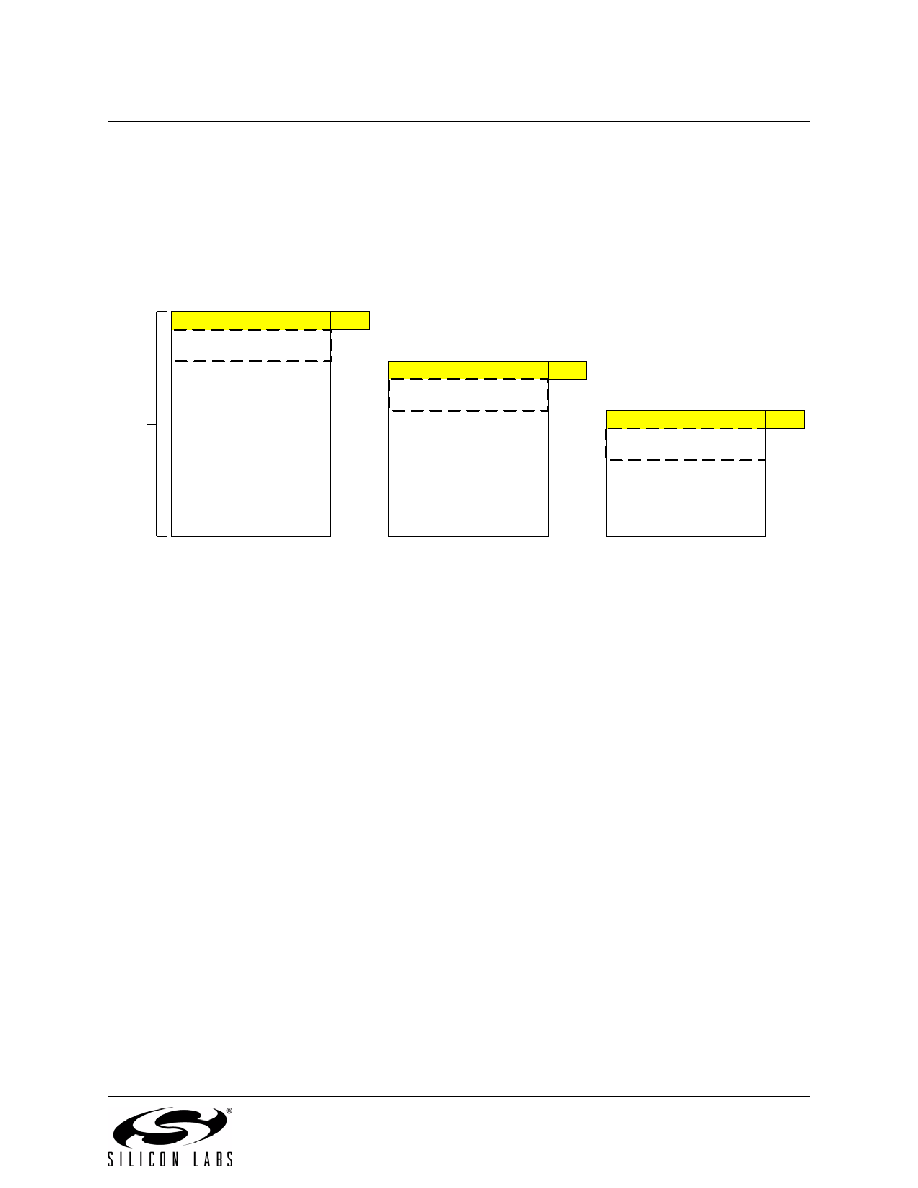
The members of the C8051F80x-83x device family contain 16 kB (C8051F80x and C8051F810/1), 8 kB
(C8051F812/3/4/5/6/7/8/9 and C8051F82x), or 4 kB (C8051F830/1/2/3/4/5) of re-programmable Flash
memory that can be used as non-volatile program or data storage. The last byte of user code space is
used as the security lock byte (0x3FFF on 16 kB devices, 0x1FFF on 8 kB devices and 0x0FFF on 4 kB
devices).
Figure 15.2. Flash Program Memory Map
15.1.1. MOVX Instruction and Program Memory
The MOVX instruction in an 8051 device is typically used to access external data memory. On the
C8051F80x-83x devices, the MOVX instruction is normally used to read and write on-chip XRAM, but can
be re-configured to write and erase on-chip Flash memory space. MOVC instructions are always used to
read Flash memory, while MOVX write instructions are used to erase and write Flash. This Flash access
feature provides a mechanism for the C8051F80x-83x to update program code and use the program mem-
ory space for non-volatile data storage. Refer to Section “19. Flash Memory” on page 113 for further
details.
15.2. Data Memory
The members of the C8051F80x-83x device family contain 512 bytes (C8051F80x, C8051F81x, and
C8051F820/1/2/3) or 256 bytes (C8051F824/5/6/7/8/9 and C8051F830/1/2/3/4/5) of RAM data memory.
For all C8051F80x-83x devices, 256 bytes of this memory is mapped into the internal RAM space of the
8051. For the devices with 512 bytes of RAM, the remaining 256 bytes of this memory is on-chip “external”
memory. The data memory map is shown in Figure 15.1 for reference.
15.2.1. Internal RAM
There are 256 bytes of internal RAM mapped into the data memory space from 0x00 through 0xFF. The
lower 128 bytes of data memory are used for general purpose registers and scratch pad memory. Either
direct or indirect addressing may be used to access the lower 128 bytes of data memory. Locations 0x00
through 0x1F are addressable as four banks of general purpose registers, each bank consisting of eight
byte-wide registers. The next 16 bytes, locations 0x20 through 0x2F, may either be addressed as bytes or
as 128 bit locations accessible with the direct addressing mode.
The upper 128 bytes of data memory are accessible only by indirect addressing. This region occupies the
same address space as the Special Function Registers (SFR) but is physically separate from the SFR
space. The addressing mode used by an instruction when accessing locations above 0x7F determines
Lock Byte
0x0000
0x3FFF
0x3FFE
F
L
A
S
H
me
mo
ry
o
rga
ni
z
e
d
i
n
512
-b
yte
page
s
0x3E00
Flash Memory Space
Lock Byte Page
Lock Byte
0x0000
0x1FFF
0x1FFE
0x1E00
Flash Memory Space
Lock Byte Page
Lock Byte
0x0000
0x0FFF
0x0FFE
0x0E00
Flash Memory Space
Lock Byte Page
C8051F80x and
C8051F810/1 (16kB)
C8051F812/3/4/5/6/7/8/9
and C8051F82x (8 kB)
C8051F830/1/2/3/4/5 (4 kB)
相关PDF资料 |
PDF描述 |
|---|---|
| UPD78F9512GR-JJG-A | MCU 8BIT SGL CHIP 16PIN |
| VI-J3D-IW-F3 | CONVERTER MOD DC/DC 85V 100W |
| C8051F826-GS | IC MCU 8BIT 8KB FLASH 16SOIC |
| VI-J3D-IW-F2 | CONVERTER MOD DC/DC 85V 100W |
| VI-J3B-IW-F4 | CONVERTER MOD DC/DC 95V 100W |
相关代理商/技术参数 |
参数描述 |
|---|---|
| C8051F820-GMR | 功能描述:8位微控制器 -MCU 8kB 512B RAM RoHS:否 制造商:Silicon Labs 核心:8051 处理器系列:C8051F39x 数据总线宽度:8 bit 最大时钟频率:50 MHz 程序存储器大小:16 KB 数据 RAM 大小:1 KB 片上 ADC:Yes 工作电源电压:1.8 V to 3.6 V 工作温度范围:- 40 C to + 105 C 封装 / 箱体:QFN-20 安装风格:SMD/SMT |
| C8051F820-GU | 功能描述:8位微控制器 -MCU 8kB, 512B RAM RoHS:否 制造商:Silicon Labs 核心:8051 处理器系列:C8051F39x 数据总线宽度:8 bit 最大时钟频率:50 MHz 程序存储器大小:16 KB 数据 RAM 大小:1 KB 片上 ADC:Yes 工作电源电压:1.8 V to 3.6 V 工作温度范围:- 40 C to + 105 C 封装 / 箱体:QFN-20 安装风格:SMD/SMT |
| C8051F820-GUR | 功能描述:8位微控制器 -MCU 8kB 512B RAM RoHS:否 制造商:Silicon Labs 核心:8051 处理器系列:C8051F39x 数据总线宽度:8 bit 最大时钟频率:50 MHz 程序存储器大小:16 KB 数据 RAM 大小:1 KB 片上 ADC:Yes 工作电源电压:1.8 V to 3.6 V 工作温度范围:- 40 C to + 105 C 封装 / 箱体:QFN-20 安装风格:SMD/SMT |
| C8051F821-GS | 功能描述:8位微控制器 -MCU 8kB, 512B RAM 12-ch CDC RoHS:否 制造商:Silicon Labs 核心:8051 处理器系列:C8051F39x 数据总线宽度:8 bit 最大时钟频率:50 MHz 程序存储器大小:16 KB 数据 RAM 大小:1 KB 片上 ADC:Yes 工作电源电压:1.8 V to 3.6 V 工作温度范围:- 40 C to + 105 C 封装 / 箱体:QFN-20 安装风格:SMD/SMT |
| C8051F821-GSR | 功能描述:8位微控制器 -MCU 8kB 512B RAM 12-CH CDC RoHS:否 制造商:Silicon Labs 核心:8051 处理器系列:C8051F39x 数据总线宽度:8 bit 最大时钟频率:50 MHz 程序存储器大小:16 KB 数据 RAM 大小:1 KB 片上 ADC:Yes 工作电源电压:1.8 V to 3.6 V 工作温度范围:- 40 C to + 105 C 封装 / 箱体:QFN-20 安装风格:SMD/SMT |
发布紧急采购,3分钟左右您将得到回复。