- 您现在的位置:买卖IC网 > PDF目录11707 > C8051F822-GS (Silicon Laboratories Inc)IC MCU 8BIT 8KB FLASH 16SOIC PDF资料下载
参数资料
| 型号: | C8051F822-GS |
| 厂商: | Silicon Laboratories Inc |
| 文件页数: | 153/250页 |
| 文件大小: | 0K |
| 描述: | IC MCU 8BIT 8KB FLASH 16SOIC |
| 产品培训模块: | Serial Communication Overview |
| 特色产品: | QuickSense? Portfolio |
| 标准包装: | 48 |
| 系列: | C8051F82x |
| 核心处理器: | 8051 |
| 芯体尺寸: | 8-位 |
| 速度: | 25MHz |
| 连通性: | SMBus(2 线/I²C),SPI,UART/USART |
| 外围设备: | 电容感应,POR,PWM,WDT |
| 输入/输出数: | 13 |
| 程序存储器容量: | 8KB(8K x 8) |
| 程序存储器类型: | 闪存 |
| RAM 容量: | 512 x 8 |
| 电压 - 电源 (Vcc/Vdd): | 1.8 V ~ 3.6 V |
| 振荡器型: | 内部 |
| 工作温度: | -40°C ~ 85°C |
| 封装/外壳: | 16-SOIC(0.154",3.90mm 宽) |
| 包装: | 管件 |
| 产品目录页面: | 625 (CN2011-ZH PDF) |
| 其它名称: | 336-1802-5 |
第1页第2页第3页第4页第5页第6页第7页第8页第9页第10页第11页第12页第13页第14页第15页第16页第17页第18页第19页第20页第21页第22页第23页第24页第25页第26页第27页第28页第29页第30页第31页第32页第33页第34页第35页第36页第37页第38页第39页第40页第41页第42页第43页第44页第45页第46页第47页第48页第49页第50页第51页第52页第53页第54页第55页第56页第57页第58页第59页第60页第61页第62页第63页第64页第65页第66页第67页第68页第69页第70页第71页第72页第73页第74页第75页第76页第77页第78页第79页第80页第81页第82页第83页第84页第85页第86页第87页第88页第89页第90页第91页第92页第93页第94页第95页第96页第97页第98页第99页第100页第101页第102页第103页第104页第105页第106页第107页第108页第109页第110页第111页第112页第113页第114页第115页第116页第117页第118页第119页第120页第121页第122页第123页第124页第125页第126页第127页第128页第129页第130页第131页第132页第133页第134页第135页第136页第137页第138页第139页第140页第141页第142页第143页第144页第145页第146页第147页第148页第149页第150页第151页第152页当前第153页第154页第155页第156页第157页第158页第159页第160页第161页第162页第163页第164页第165页第166页第167页第168页第169页第170页第171页第172页第173页第174页第175页第176页第177页第178页第179页第180页第181页第182页第183页第184页第185页第186页第187页第188页第189页第190页第191页第192页第193页第194页第195页第196页第197页第198页第199页第200页第201页第202页第203页第204页第205页第206页第207页第208页第209页第210页第211页第212页第213页第214页第215页第216页第217页第218页第219页第220页第221页第222页第223页第224页第225页第226页第227页第228页第229页第230页第231页第232页第233页第234页第235页第236页第237页第238页第239页第240页第241页第242页第243页第244页第245页第246页第247页第248页第249页第250页
C8051F80x-83x
236
Rev. 1.0
29.4. Watchdog Timer Mode
A programmable watchdog timer (WDT) function is available through the PCA Module 2. The WDT is used
to generate a reset if the time between writes to the WDT update register (PCA0CPH2) exceed a specified
limit. The WDT can be configured and enabled/disabled as needed by software.
With the WDTE bit set in the PCA0MD register, Module 2 operates as a watchdog timer (WDT). The Mod-
ule 2 high byte is compared to the PCA counter high byte; the Module 2 low byte holds the offset to be
used when WDT updates are performed. The Watchdog Timer is enabled on reset. Writes to some
PCA registers are restricted while the Watchdog Timer is enabled. The WDT will generate a reset
shortly after code begins execution. To avoid this reset, the WDT should be explicitly disabled (and option-
ally re-configured and re-enabled if it is used in the system).
29.4.1. Watchdog Timer Operation
While the WDT is enabled:
PCA counter is forced on.
Writes to PCA0L and PCA0H are not allowed.
PCA clock source bits (CPS2–CPS0) are frozen.
PCA Idle control bit (CIDL) is frozen.
Module 2 is forced into software timer mode.
Writes to the Module 2 mode register (PCA0CPM2) are disabled.
While the WDT is enabled, writes to the CR bit will not change the PCA counter state; the counter will run
until the WDT is disabled. The PCA counter run control bit (CR) will read zero if the WDT is enabled but
user software has not enabled the PCA counter. If a match occurs between PCA0CPH2 and PCA0H while
the WDT is enabled, a reset will be generated. To prevent a WDT reset, the WDT may be updated with a
write of any value to PCA0CPH2. Upon a PCA0CPH2 write, PCA0H plus the offset held in PCA0CPL2 is
loaded into PCA0CPH2 (See Figure 29.11).
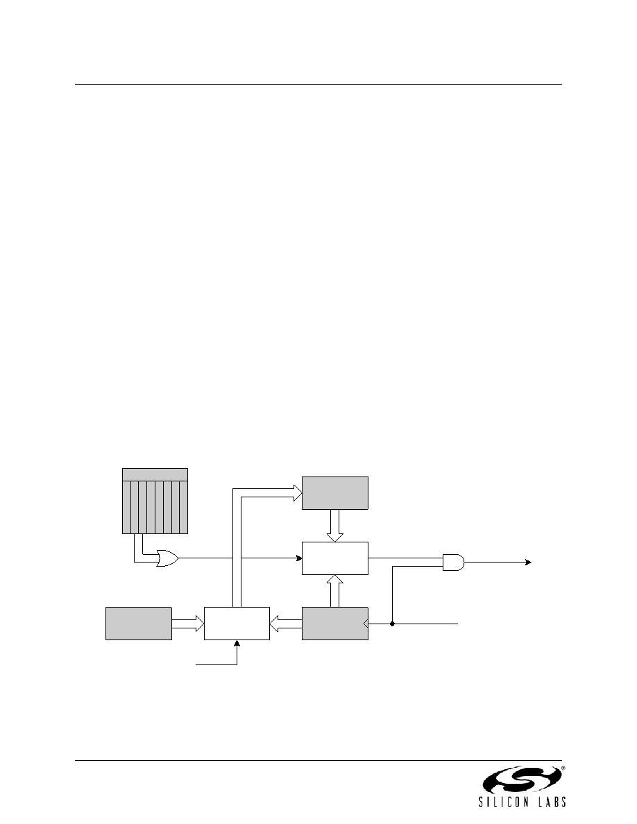
Figure 29.11. PCA Module 2 with Watchdog Timer Enabled
The 8-bit offset held in PCA0CPH2 is compared to the upper byte of the 16-bit PCA counter. This offset
value is the number of PCA0L overflows before a reset. Up to 256 PCA clocks may pass before the first
PCA0L overflow occurs, depending on the value of the PCA0L when the update is performed. The total off-
PCA0H
Enable
PCA0L Overflow
Reset
PCA0CPL2
8-bit Adder
PCA0CPH2
Adder
Enable
PCA0MD
C
I
D
L
W
D
T
E
C
F
C
P
S
1
C
P
S
0
W
D
L
C
K
C
P
S
2
Match
Write to
PCA0CPH2
8-bit
Comparator
相关PDF资料 |
PDF描述 |
|---|---|
| MS27467E17B99SA | CONN PLUG 23POS STRAIGHT W/SCKT |
| C8051F819-GM | IC MCU 8BIT 8KB FLASH 20QFN |
| D38999/26WF11SN | CONN PLUG 11POS STRAIGHT W/SCKT |
| VE-J51-IW-F1 | CONVERTER MOD DC/DC 12V 100W |
| MS27466T25B29P | CONN RCPT 29POS WALL MT W/PINS |
相关代理商/技术参数 |
参数描述 |
|---|---|
| C8051F822-GSR | 功能描述:8位微控制器 -MCU 8kB 512B RAM 8-CH CDC RoHS:否 制造商:Silicon Labs 核心:8051 处理器系列:C8051F39x 数据总线宽度:8 bit 最大时钟频率:50 MHz 程序存储器大小:16 KB 数据 RAM 大小:1 KB 片上 ADC:Yes 工作电源电压:1.8 V to 3.6 V 工作温度范围:- 40 C to + 105 C 封装 / 箱体:QFN-20 安装风格:SMD/SMT |
| C8051F823-GS | 功能描述:8位微控制器 -MCU 8kB, 512B RAM RoHS:否 制造商:Silicon Labs 核心:8051 处理器系列:C8051F39x 数据总线宽度:8 bit 最大时钟频率:50 MHz 程序存储器大小:16 KB 数据 RAM 大小:1 KB 片上 ADC:Yes 工作电源电压:1.8 V to 3.6 V 工作温度范围:- 40 C to + 105 C 封装 / 箱体:QFN-20 安装风格:SMD/SMT |
| C8051F823-GSR | 功能描述:8位微控制器 -MCU 8kB 512B RAM RoHS:否 制造商:Silicon Labs 核心:8051 处理器系列:C8051F39x 数据总线宽度:8 bit 最大时钟频率:50 MHz 程序存储器大小:16 KB 数据 RAM 大小:1 KB 片上 ADC:Yes 工作电源电压:1.8 V to 3.6 V 工作温度范围:- 40 C to + 105 C 封装 / 箱体:QFN-20 安装风格:SMD/SMT |
| C8051F824-GS | 功能描述:8位微控制器 -MCU 8kB, 256B RAM, ADC 12-ch CDC RoHS:否 制造商:Silicon Labs 核心:8051 处理器系列:C8051F39x 数据总线宽度:8 bit 最大时钟频率:50 MHz 程序存储器大小:16 KB 数据 RAM 大小:1 KB 片上 ADC:Yes 工作电源电压:1.8 V to 3.6 V 工作温度范围:- 40 C to + 105 C 封装 / 箱体:QFN-20 安装风格:SMD/SMT |
| C8051F824-GSR | 功能描述:8位微控制器 -MCU 8kB 256B RAM ADC 12-CH CDC RoHS:否 制造商:Silicon Labs 核心:8051 处理器系列:C8051F39x 数据总线宽度:8 bit 最大时钟频率:50 MHz 程序存储器大小:16 KB 数据 RAM 大小:1 KB 片上 ADC:Yes 工作电源电压:1.8 V to 3.6 V 工作温度范围:- 40 C to + 105 C 封装 / 箱体:QFN-20 安装风格:SMD/SMT |
发布紧急采购,3分钟左右您将得到回复。