- 您现在的位置:买卖IC网 > PDF目录3796 > C8051F931-GM (Silicon Laboratories Inc)IC 8051 MCU 64K FLASH 24-QFN PDF资料下载
参数资料
| 型号: | C8051F931-GM |
| 厂商: | Silicon Laboratories Inc |
| 文件页数: | 171/330页 |
| 文件大小: | 0K |
| 描述: | IC 8051 MCU 64K FLASH 24-QFN |
| 产品培训模块: | C8051F9xx Lower Power MCUs Serial Communication Overview |
| 视频文件: | Designing for Low Power Operation |
| 特色产品: | C8051F91x/0x MCU Series Development Kit |
| 标准包装: | 91 |
| 系列: | C8051F9xx |
| 核心处理器: | 8051 |
| 芯体尺寸: | 8-位 |
| 速度: | 25MHz |
| 连通性: | SMBus(2 线/I²C),SPI,UART/USART |
| 外围设备: | 欠压检测/复位,POR,PWM,温度传感器,WDT |
| 输入/输出数: | 16 |
| 程序存储器容量: | 64KB(64K x 8) |
| 程序存储器类型: | 闪存 |
| RAM 容量: | 4.25K x 8 |
| 电压 - 电源 (Vcc/Vdd): | 0.9 V ~ 3.6 V |
| 数据转换器: | A/D 15x10b |
| 振荡器型: | 内部 |
| 工作温度: | -40°C ~ 85°C |
| 封装/外壳: | 24-WFQFN 裸露焊盘 |
| 包装: | 托盘 |
| 产品目录页面: | 625 (CN2011-ZH PDF) |
| 配用: | 336-1479-ND - PLATFORM PROG TOOLSTCK F921,F931 336-1476-ND - DAUGHTER CARD CAP TOUCH SENSE 336-1475-ND - KIT STARTER CAP TOUCH SENSE 336-1474-ND - DAUGHTER CARD TOOLSTCK C8051F931 336-1473-ND - KIT DEV C8051F920,F921,F930,F931 |
| 其它名称: | 336-1468 |
第1页第2页第3页第4页第5页第6页第7页第8页第9页第10页第11页第12页第13页第14页第15页第16页第17页第18页第19页第20页第21页第22页第23页第24页第25页第26页第27页第28页第29页第30页第31页第32页第33页第34页第35页第36页第37页第38页第39页第40页第41页第42页第43页第44页第45页第46页第47页第48页第49页第50页第51页第52页第53页第54页第55页第56页第57页第58页第59页第60页第61页第62页第63页第64页第65页第66页第67页第68页第69页第70页第71页第72页第73页第74页第75页第76页第77页第78页第79页第80页第81页第82页第83页第84页第85页第86页第87页第88页第89页第90页第91页第92页第93页第94页第95页第96页第97页第98页第99页第100页第101页第102页第103页第104页第105页第106页第107页第108页第109页第110页第111页第112页第113页第114页第115页第116页第117页第118页第119页第120页第121页第122页第123页第124页第125页第126页第127页第128页第129页第130页第131页第132页第133页第134页第135页第136页第137页第138页第139页第140页第141页第142页第143页第144页第145页第146页第147页第148页第149页第150页第151页第152页第153页第154页第155页第156页第157页第158页第159页第160页第161页第162页第163页第164页第165页第166页第167页第168页第169页第170页当前第171页第172页第173页第174页第175页第176页第177页第178页第179页第180页第181页第182页第183页第184页第185页第186页第187页第188页第189页第190页第191页第192页第193页第194页第195页第196页第197页第198页第199页第200页第201页第202页第203页第204页第205页第206页第207页第208页第209页第210页第211页第212页第213页第214页第215页第216页第217页第218页第219页第220页第221页第222页第223页第224页第225页第226页第227页第228页第229页第230页第231页第232页第233页第234页第235页第236页第237页第238页第239页第240页第241页第242页第243页第244页第245页第246页第247页第248页第249页第250页第251页第252页第253页第254页第255页第256页第257页第258页第259页第260页第261页第262页第263页第264页第265页第266页第267页第268页第269页第270页第271页第272页第273页第274页第275页第276页第277页第278页第279页第280页第281页第282页第283页第284页第285页第286页第287页第288页第289页第290页第291页第292页第293页第294页第295页第296页第297页第298页第299页第300页第301页第302页第303页第304页第305页第306页第307页第308页第309页第310页第311页第312页第313页第314页第315页第316页第317页第318页第319页第320页第321页第322页第323页第324页第325页第326页第327页第328页第329页第330页
C8051F93x-C8051F92x
252
Rev. 1.4
22.5. SMBus Transfer Modes
The SMBus interface may be configured to operate as master and/or slave. At any particular time, it will be
operating in one of the following four modes: Master Transmitter, Master Receiver, Slave Transmitter, or
Slave Receiver. The SMBus interface enters Master Mode any time a START is generated, and remains in
Master Mode until it loses an arbitration or generates a STOP. An SMBus interrupt is generated at the end
of all SMBus byte frames. Note that the position of the ACK interrupt when operating as a receiver
depends on whether hardware ACK generation is enabled. As a receiver, the interrupt for an ACK occurs
before
the ACK with hardware ACK generation disabled, and after the ACK when hardware ACK
generation is enabled. As a transmitter, interrupts occur after the ACK, regardless of whether hardware
ACK generation is enabled or not.
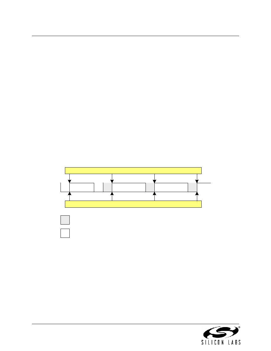
22.5.1. Write Sequence (Master)
During a write sequence, an SMBus master writes data to a slave device. The master in this transfer will be
a transmitter during the address byte, and a transmitter during all data bytes. The SMBus interface
generates the START condition and transmits the first byte containing the address of the target slave and
the data direction bit. In this case the data direction bit (R/W) will be logic 0 (WRITE). The master then
transmits one or more bytes of serial data. After each byte is transmitted, an acknowledge bit is generated
by the slave. The transfer is ended when the STO bit is set and a STOP is generated. Note that the
interface will switch to Master Receiver Mode if SMB0DAT is not written following a Master Transmitter
interrupt. Figure 22.5 shows a typical master write sequence. Two transmit data bytes are shown, though
any number of bytes may be transmitted. All “data byte transferred” interrupts occur after the ACK cycle in
this mode, regardless of whether hardware ACK generation is enabled.
Figure 22.5. Typical Master Write Sequence
A
S
W
P
Data Byte
SLA
S = START
P = STOP
A = ACK
W = WRITE
SLA = Slave Address
Received by SMBus
Interface
Transmitted by
SMBus Interface
Interrupts with Hardware ACK Disabled (EHACK = 0)
Interrupts with Hardware ACK Enabled (EHACK = 1)
相关PDF资料 |
PDF描述 |
|---|---|
| P87LPC762FD,512 | IC 80C51 MCU 2K OTP 20-SOIC |
| MC68HC908JK3CP | IC MCU 8MHZ 4K FLASH 20-DIP |
| MC68HC908JK3CDW | IC MCU 8MHZ 4K FLASH 20-SOIC |
| MC68HC908JK1CP | IC MCU 8MHZ 1.5K FLASH 20-DIP |
| MC68HC908JK1CDW | IC MCU 8MHZ 1.5K FLASH 20-SOIC |
相关代理商/技术参数 |
参数描述 |
|---|---|
| C8051F931-GMR | 功能描述:8位微控制器 -MCU 64KB 10ADC MCU LEAD FREE RoHS:否 制造商:Silicon Labs 核心:8051 处理器系列:C8051F39x 数据总线宽度:8 bit 最大时钟频率:50 MHz 程序存储器大小:16 KB 数据 RAM 大小:1 KB 片上 ADC:Yes 工作电源电压:1.8 V to 3.6 V 工作温度范围:- 40 C to + 105 C 封装 / 箱体:QFN-20 安装风格:SMD/SMT |
| C8051F93X | 制造商:未知厂家 制造商全称:未知厂家 功能描述:Single/Dual Battery, 0.9–3.6 V, 64/32 kB, smaRTClock, 10-Bit ADC MCU |
| C8051F960-A-DK | 功能描述:开发板和工具包 - 8051 C8051F96X Development Kit RoHS:否 制造商:Silicon Labs 产品:Development Kits 工具用于评估:C8051F960, Si7005 核心: 接口类型:USB 工作电源电压: |
| C8051F960-A-GM | 功能描述:8位微控制器 -MCU 128KB, DC-DC, LCD AES, DQFN76 RoHS:否 制造商:Silicon Labs 核心:8051 处理器系列:C8051F39x 数据总线宽度:8 bit 最大时钟频率:50 MHz 程序存储器大小:16 KB 数据 RAM 大小:1 KB 片上 ADC:Yes 工作电源电压:1.8 V to 3.6 V 工作温度范围:- 40 C to + 105 C 封装 / 箱体:QFN-20 安装风格:SMD/SMT |
| C8051F960-A-GMR | 制造商:Silicon Laboratories Inc 功能描述:128KB, DC-DC, LCD, AES, DQFN76 - Tape and Reel 制造商:Silicon Laboratories Inc 功能描述:IC MCU 128KB DC-DC LCDAES 76DQFN |
发布紧急采购,3分钟左右您将得到回复。