参数资料
| 型号: | CA3140AMZ96 |
| 厂商: | Intersil |
| 文件页数: | 5/23页 |
| 文件大小: | 0K |
| 描述: | IC OP AMP 4.5MHZ BIMOS 8-SOIC |
| 标准包装: | 1 |
| 放大器类型: | 通用 |
| 电路数: | 1 |
| 转换速率: | 9 V/µs |
| 增益带宽积: | 4.5MHz |
| 电流 - 输入偏压: | 10pA |
| 电压 - 输入偏移: | 2000µV |
| 电流 - 电源: | 4mA |
| 电流 - 输出 / 通道: | 40mA |
| 电压 - 电源,单路/双路(±): | 4 V ~ 36 V,±2 V ~ 18 V |
| 工作温度: | -50°C ~ 125°C |
| 安装类型: | 表面贴装 |
| 封装/外壳: | 8-SOIC(0.154",3.90mm 宽) |
| 供应商设备封装: | 8-SOIC |
| 包装: | 标准包装 |
| 其它名称: | CA3140AMZ96DKR |
13
FN957.10
July 11, 2005
This circuit can be adjusted most easily with a distortion
analyzer, but a good first approximation can be made by
comparing the output signal with that of a sine wave
generator. The initial slope is adjusted with the potentiometer
R1, followed by an adjustment of R2. The final slope is
established by adjusting R3, thereby adding additional
segments that are contributed by these diodes. Because
there is some interaction among these controls, repetition of
the adjustment procedure may be necessary.
Sweeping Generator
Figure 13 shows a sweeping generator. Three CA3140s are
used in this circuit. One CA3140 is used as an integrator, a
second device is used as a hysteresis switch that determines
the starting and stopping points of the sweep. A third
CA3140 is used as a logarithmic shaping network for the log
function. Rates and slopes, as well as sawtooth, triangle,
and logarithmic sweeps are generated by this circuit.
Wideband Output Amplifier
Figure 14 shows a high slew rate, wideband amplifier
suitable for use as a 50
transmission line driver. This
circuit, when used in conjunction with the function generator
and sine wave shaper circuits shown in Figures 10 and 12
provides 18VP-P output open circuited, or 9VP-P output
when terminated in 50
. The slew rate required of this
amplifier is 28V/
s (18V
P-P x π x 0.5MHz).
Power Supplies
High input impedance, common mode capability down to the
negative supply and high output drive current capability are
key factors in the design of wide range output voltage
supplies that use a single input voltage to provide a
regulated output voltage that can be adjusted from
essentially 0V to 24V.
Unlike many regulator systems using comparators having a
bipolar transistor input stage, a high impedance reference
voltage divider from a single supply can be used in
connection with the CA3140 (see Figure 15).
Essentially, the regulators, shown in Figures 16 and 17, are
connected as non inverting power operational amplifiers with a
gain of 3.2. An 8V reference input yields a maximum output
voltage slightly greater than 25V. As a voltage follower, when
the reference input goes to 0V the output will be 0V. Because
the offset voltage is also multiplied by the 3.2 gain factor, a
potentiometer is needed to null the offset voltage.
Series pass transistors with high ICBO levels will also
prevent the output voltage from reaching zero because there
is a finite voltage drop (VCESAT) across the output of the
CA3140 (see Figure 2). This saturation voltage level may
indeed set the lowest voltage obtainable.
The high impedance presented by Terminal 8 is
advantageous in effecting current limiting. Thus, only a small
signal transistor is required for the current-limit sensing
amplifier. Resistive decoupling is provided for this transistor
to minimize damage to it or the CA3140 in the event of
unusual input or output transients on the supply rail.
Figures 16 and 17, show circuits in which a D2201 high speed
diode is used for the current sensor. This diode was chosen
for its slightly higher forward voltage drop characteristic, thus
giving greater sensitivity. It must be emphasized that heat
sinking of this diode is essential to minimize variation of the
current trip point due to internal heating of the diode. That is,
1A at 1V forward drop represents one watt which can result in
significant regenerative changes in the current trip point as the
diode temperature rises. Placing the small signal reference
amplifier in the proximity of the current sensing diode also
helps minimize the variability in the trip level due to the
negative temperature coefficient of the diode. In spite of those
limitations, the current limiting point can easily be adjusted
over the range from 10mA to 1A with a single adjustment
potentiometer. If the temperature stability of the current
limiting system is a serious consideration, the more usual
current sampling resistor type of circuitry should be employed.
A power Darlington transistor (in a metal can with heatsink),
is used as the series pass element for the conventional
current limiting system, Figure 16, because high power
Darlington dissipation will be encountered at low output
voltage and high currents.
2
6
8
1
4
7
+
CA3140
-
50
F
25V
2.2
k
2N3053
1N914
2.2
k
1N914
2.7
2.7
2N4037
+
-
+
- 50F
25V
3
SIGNAL
LEVEL
ADJUSTMENT
2.5k
200
2.4pF
2pF
-15V
+15V
OUTPUT
DC LEVEL
ADJUSTMENT
-15V
+15V
3k
200
1.8k
51
2W
OUT
NOMINAL BANDWIDTH = 10MHz
tr = 35ns
FIGURE 14. WIDEBAND OUTPUT AMPLIFIER
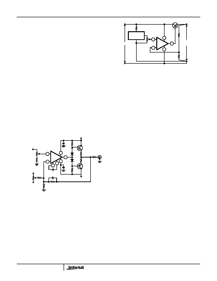
6
3
2
4
7
+
CA3140
-
VOLTAGE
REFERENCE
VOLTAGE
ADJUSTMENT
REGULATED
OUTPUT
INPUT
FIGURE 15. BASIC SINGLE SUPPLY VOLTAGE REGULATOR
SHOWING VOLTAGE FOLLOWER CONFIGURATION
CA3140, CA3140A
相关PDF资料 |
PDF描述 |
|---|---|
| 3431-6502UG | CONN HEADER 34PS STR SHORT LATCH |
| 3429-2602UG | CONN HEADER 26POS STR LONG LATCH |
| 3429-2502UG | CONN HEADER 26PS STR SHORT LATCH |
| 65863-213 | QKE HDR 2X30 |
| DIN-096CSC-R1L-KR | CONN DIN SOCKET 96POS VERT GOLD |
相关代理商/技术参数 |
参数描述 |
|---|---|
| CA3140AS | 制造商:INTERSIL 制造商全称:Intersil Corporation 功能描述:4.5MHz, BiMOS Operational Amplifier with MOSFET Input/Bipolar Output |
| CA3140AT | 制造商:Harris Corporation 功能描述: 制造商:Rochester Electronics LLC 功能描述: |
| CA3140BT | 制造商:未知厂家 制造商全称:未知厂家 功能描述:BiMOS Operational Amplifier with MOSFET Input/Bipolar Output(886.70 k) |
| CA3140E | 功能描述:IC OPAMP DUAL BIMOS 4.5MHZ 8-DIP RoHS:否 类别:集成电路 (IC) >> Linear - Amplifiers - Instrumentation 系列:- 标准包装:1,000 系列:- 放大器类型:电压反馈 电路数:4 输出类型:满摆幅 转换速率:33 V/µs 增益带宽积:20MHz -3db带宽:30MHz 电流 - 输入偏压:2nA 电压 - 输入偏移:3000µV 电流 - 电源:2.5mA 电流 - 输出 / 通道:30mA 电压 - 电源,单路/双路(±):4.5 V ~ 16.5 V,±2.25 V ~ 8.25 V 工作温度:-40°C ~ 85°C 安装类型:表面贴装 封装/外壳:14-SOIC(0.154",3.90mm 宽) 供应商设备封装:14-SOIC 包装:带卷 (TR) |
| CA3140E | 制造商:Intersil Corporation 功能描述:IC OP-AMP SINGLE 8PDIP |
发布紧急采购,3分钟左右您将得到回复。