参数资料
| 型号: | CA3140E |
| 厂商: | Intersil |
| 文件页数: | 17/23页 |
| 文件大小: | 0K |
| 描述: | IC OPAMP DUAL BIMOS 4.5MHZ 8-DIP |
| 标准包装: | 50 |
| 放大器类型: | 通用 |
| 电路数: | 1 |
| 转换速率: | 9 V/µs |
| 增益带宽积: | 4.5MHz |
| 电流 - 输入偏压: | 10pA |
| 电压 - 输入偏移: | 5000µV |
| 电流 - 电源: | 4mA |
| 电流 - 输出 / 通道: | 40mA |
| 电压 - 电源,单路/双路(±): | 4 V ~ 36 V,±2 V ~ 18 V |
| 工作温度: | -55°C ~ 125°C |
| 安装类型: | 通孔 |
| 封装/外壳: | 8-DIP(0.300",7.62mm) |
| 供应商设备封装: | 8-PDIP |
| 包装: | 管件 |
| 其它名称: | CA3140 |
3
FN957.10
July 11, 2005
Absolute Maximum Ratings
Thermal Information
DC Supply Voltage (Between V+ and V- Terminals) . . . . . . . . . 36V
Differential Mode Input Voltage . . . . . . . . . . . . . . . . . . . . . . . . . . 8V
DC Input Voltage . . . . . . . . . . . . . . . . . . . . . . (V+ +8V) To (V- -0.5V)
Input Terminal Current . . . . . . . . . . . . . . . . . . . . . . . . . . . . . . . . 1mA
Output Short Circuit Duration
∞ (Note 2) . . . . . . . . . . . . . . Indefinite
Operating Conditions
Temperature Range . . . . . . . . . . . . . . . . . . . . . . . . . -55oC to 125oC
Thermal Resistance (Typical, Note 1)
θJA (oC/W) θJC (oC/W)
PDIP Package*. . . . . . . . . . . . . . . . . . .
115
N/A
SOIC Package . . . . . . . . . . . . . . . . . . .
165
N/A
Maximum Junction Temperature (Plastic Package) . . . . . . . 150oC
Maximum Storage Temperature Range . . . . . . . . . . -65oC to 150oC
Maximum Lead Temperature (Soldering 10s) . . . . . . . . . . . . 300oC
(SOIC - Lead Tips Only)
*Pb-free PDIPs can be used for through hole wave solder process-
ing only. They are not intended for use in Reflow solder processing
applications.
CAUTION: Stresses above those listed in “Absolute Maximum Ratings” may cause permanent damage to the device. This is a stress only rating and operation of the
device at these or any other conditions above those indicated in the operational sections of this specification is not implied.
NOTES:
1.
θ
JA is measured with the component mounted on a low effective thermal conductivity test board in free air. See Tech Brief TB379 for details
2. Short circuit may be applied to ground or to either supply.
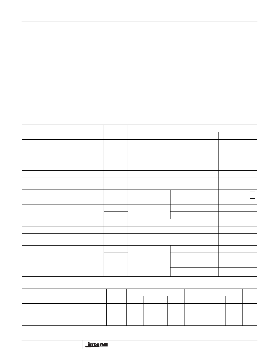
Electrical Specifications
VSUPPLY = ±15V, TA = 25
oC
PARAMETER
SYMBOL
TEST CONDITIONS
TYPICAL VALUES
UNITS
CA3140
CA3140A
Input Offset Voltage Adjustment Resistor
Typical Value of Resistor
Between Terminals 4 and 5 or 4 and 1 to
Adjust Max VIO
4.7
18
k
Input Resistance
RI
1.5
T
Input Capacitance
CI
44
pF
Output Resistance
RO
60
Equivalent Wideband Input Noise Voltage
(See Figure 27)
eN
BW = 140kHz, RS = 1M
48
V
Equivalent Input Noise Voltage (See Figure 35)
eN
RS = 100
f = 1kHz
40
nV/
√Hz
f = 10kHz
12
nV/
√Hz
Short Circuit Current to Opposite Supply
IOM+
Source
40
mA
IOM-Sink
18
mA
Gain-Bandwidth Product, (See Figures 6, 30)
fT
4.5
MHz
Slew Rate, (See Figure 31)
SR
9
V/
s
Sink Current From Terminal 8 To Terminal 4 to
Swing Output Low
220
A
Transient Response (See Figure 28)
tr
RL = 2k
CL = 100pF
Rise Time
0.08
s
OS
Overshoot
10
%
Settling Time at 10VP-P, (See Figure 5)
tS
RL = 2k
CL = 100pF
Voltage Follower
To 1mV
4.5
s
To 10mV
1.4
s
Electrical Specifications
For Equipment Design, at VSUPPLY = ±15V, TA = 25
oC, Unless Otherwise Specified
PARAMETER
SYMBOL
CA3140
CA3140A
UNITS
MIN
TYP
MAX
MIN
TYP
MAX
Input Offset Voltage
|VIO|-
5
15
-
2
5
mV
Input Offset Current
|IIO|
-
0.5
30
-
0.5
20
pA
Input Current
II
-
10
50
-
10
40
pA
CA3140, CA3140A
相关PDF资料 |
PDF描述 |
|---|---|
| SA43AG | TVS ZENER UNIDIR 500W 43V AXIAL |
| CA3130E | IC OPAMP BIMOS SGL 15MHZ 8-DIP |
| SA40ARLG | TVS ZENER UNIDIR 500W 40V AXIAL |
| LTR18EZPF5100 | RES 510 OHM 1/2W 1% 1206 WIDE |
| LTR18EZPF2701 | RES 2.70K OHM 1/2W 1% 1206 WIDE |
相关代理商/技术参数 |
参数描述 |
|---|---|
| CA3140E | 制造商:Intersil Corporation 功能描述:IC OP-AMP SINGLE 8PDIP |
| CA3140E/TEST/ABB | 制造商:Intersil Corporation 功能描述:- Rail/Tube |
| CA3140ES2357 | 制造商:Rochester Electronics LLC 功能描述:- Bulk |
| CA3140EX | 制造商:Rochester Electronics LLC 功能描述:BIMOS OP AMP MOSFET IN/BIP OUT BURN-IN 8 PDIP COM - Bulk |
| CA3140EZ | 功能描述:运算放大器 - 运放 W/ANNEAL OPAMP 4.5MH ZLWBIAS0.04NA8PDIPML RoHS:否 制造商:STMicroelectronics 通道数量:4 共模抑制比(最小值):63 dB 输入补偿电压:1 mV 输入偏流(最大值):10 pA 工作电源电压:2.7 V to 5.5 V 安装风格:SMD/SMT 封装 / 箱体:QFN-16 转换速度:0.89 V/us 关闭:No 输出电流:55 mA 最大工作温度:+ 125 C 封装:Reel |
发布紧急采购,3分钟左右您将得到回复。