参数资料
| 型号: | CA3240E |
| 厂商: | Intersil |
| 文件页数: | 12/15页 |
| 文件大小: | 0K |
| 描述: | IC OPAMP DUAL BIMOS 4.5MHZ 8-DIP |
| 标准包装: | 50 |
| 放大器类型: | 通用 |
| 电路数: | 2 |
| 转换速率: | 9 V/µs |
| 增益带宽积: | 4.5MHz |
| 电流 - 输入偏压: | 10pA |
| 电压 - 输入偏移: | 5000µV |
| 电流 - 电源: | 8mA |
| 电流 - 输出 / 通道: | 40mA |
| 电压 - 电源,单路/双路(±): | 4 V ~ 36 V,±2 V ~ 18 V |
| 工作温度: | -40°C ~ 85°C |
| 安装类型: | 通孔 |
| 封装/外壳: | 8-DIP(0.300",7.62mm) |
| 供应商设备封装: | 8-PDIP |
| 包装: | 管件 |
| 其它名称: | CA3240 |
6
FN1050.6
March 4, 2005
Application Information
Circuit Description
The schematic diagram details one amplifier section of the
CA3240. It consists of a differential amplifier stage using PMOS
transistors (Q9 and Q10) with gate-to-source protection against
static discharge damage provided by zener diodes D3, D4, and
D5. Constant current bias is applied to the differential amplifier
from transistors Q2 and Q5 connected as a constant current
source. This assures a high common-mode rejection ratio. The
output of the differential amplifier is coupled to the base of gain
stage transistor Q13 by means of an NPN current mirror that
supplies the required differential-to-single-ended conversion.
The gain stage transistor Q13 has a high impedance active
load (Q3 and Q4) to provide maximum open-loop gain. The
collector of Q13 directly drives the base of the compound
emitter-follower output stage. Pulldown for the output stage is
provided by two independent circuits: (1) constant-current-
connected transistors Q14 and Q15 and (2) dynamic current-
sink transistor Q16 and its associated circuitry. The level of
pulldown current is constant at about 1mA for Q15 and varies
from 0 to 18mA for Q16 depending on the magnitude of the
voltage between the output terminal and V+. The dynamic
current sink becomes active whenever the output terminal is
more negative than V+ by about 15V. When this condition
exists, transistors Q21 and Q16 are turned on causing Q16 to
sink current from the output terminal to V-. This current always
flows when the output is in the linear region, either from the
load resistor or from the emitter of Q18 if no load resistor is
present. The purpose of this dynamic sink is to permit the
output to go within 0.2V (VCE (sat)) of V- with a 2kΩ load to
ground. When the load is returned to V+, it may be necessary
to supplement the 1mA of current from Q15 in order to turn on
the dynamic current sink (Q16). This may be accomplished by
placing a resistor (Approx. 2k
Ω) between the output and V-.
Output Circuit Considerations
Figure 23 shows output current-sinking capabilities of the
CA3240 at various supply voltages. Output voltage swing to
the negative supply rail permits this device to operate both
power transistors and thyristors directly without the need for
level-shifting circuitry usually associated with the 741 series
of operational amplifiers.
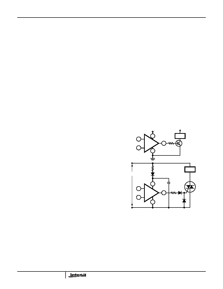
Figure 3 shows some typical configurations. Note that a series
resistor, RL, is used in both cases to limit the drive available to
the driven device. Moreover, it is recommended that a series
diode and shunt diode be used at the thyristor input to prevent
large negative transient surges that can appear at the gate of
thyristors, from damaging the integrated circuit.
Input Circuit Considerations
As indicated by the typical VICR, this device will accept
inputs as low as 0.5V below V-. However, a series current-
limiting resistor is recommended to limit the maximum input
terminal current to less than 1mA to prevent damage to the
input protection circuitry.
Moreover, some current-limiting resistance should be
provided between the inverting input and the output when
the CA3240 is used as a unity-gain voltage follower. This
resistance prevents the possibility of extremely large input-
signal transients from forcing a signal through the input-
protection network and directly driving the internal constant-
current source which could result in positive feedback via the
output terminal. A 3.9k
Ω resistor is sufficient.
The typical input current is on the order of 10pA when the
inputs are centered at nominal device dissipation. As the
output supplies load current, device dissipation will increase,
raising the chip temperature and resulting in increased input
current. Figure 4 shows typical input-terminal current versus
ambient temperature for the CA3240.
CA3240
RS
RL
MT1
MT2
120VAC
LOAD
30V NO LOAD
CA3240
LOAD
RL
V+
+HV
FIGURE 3. METHODS OF UTILIZING THE VCE (SAT) SINKING
CURRENT CAPABILITY OF THE CA3240 SERIES
CA3240, CA3240A
相关PDF资料 |
PDF描述 |
|---|---|
| 1-207532-0 | CONN HEADER SKT 24POS VERT GOLD |
| CA3140E | IC OPAMP DUAL BIMOS 4.5MHZ 8-DIP |
| SA43AG | TVS ZENER UNIDIR 500W 43V AXIAL |
| CA3130E | IC OPAMP BIMOS SGL 15MHZ 8-DIP |
| SA40ARLG | TVS ZENER UNIDIR 500W 40V AXIAL |
相关代理商/技术参数 |
参数描述 |
|---|---|
| CA3240E1 | 制造商:未知厂家 制造商全称:未知厂家 功能描述:IC-DUAL OP AMP |
| CA3240EX | 制造商:Rochester Electronics LLC 功能描述:BIMOS DUAL OP AMP MOSFET IN BIP OUT BURN-IN 8 PDIP COM - Bulk |
| CA3240EZ | 功能描述:运算放大器 - 运放 OPAMP 2X 4.5MHZ LWBI AS 0.05NA 8PDIP RoHS:否 制造商:STMicroelectronics 通道数量:4 共模抑制比(最小值):63 dB 输入补偿电压:1 mV 输入偏流(最大值):10 pA 工作电源电压:2.7 V to 5.5 V 安装风格:SMD/SMT 封装 / 箱体:QFN-16 转换速度:0.89 V/us 关闭:No 输出电流:55 mA 最大工作温度:+ 125 C 封装:Reel |
| CA3240R2188 | 制造商:Harris Corporation 功能描述: |
| CA3240T | 制造商:未知厂家 制造商全称:未知厂家 功能描述:Analog IC |
发布紧急采购,3分钟左右您将得到回复。