- 您现在的位置:买卖IC网 > PDF目录298899 > CAT1161PI-45 I2C Serial EEPROM with Supervisory Features PDF资料下载
参数资料
| 型号: | CAT1161PI-45 |
| 元件分类: | EEPROM |
| 英文描述: | I2C Serial EEPROM with Supervisory Features |
| 中文描述: | I2C串行EEPROM,带有监控功能 |
| 文件页数: | 6/12页 |
| 文件大小: | 71K |
| 代理商: | CAT1161PI-45 |
3
CAT1161/2
Doc No. 3002, Rev. C
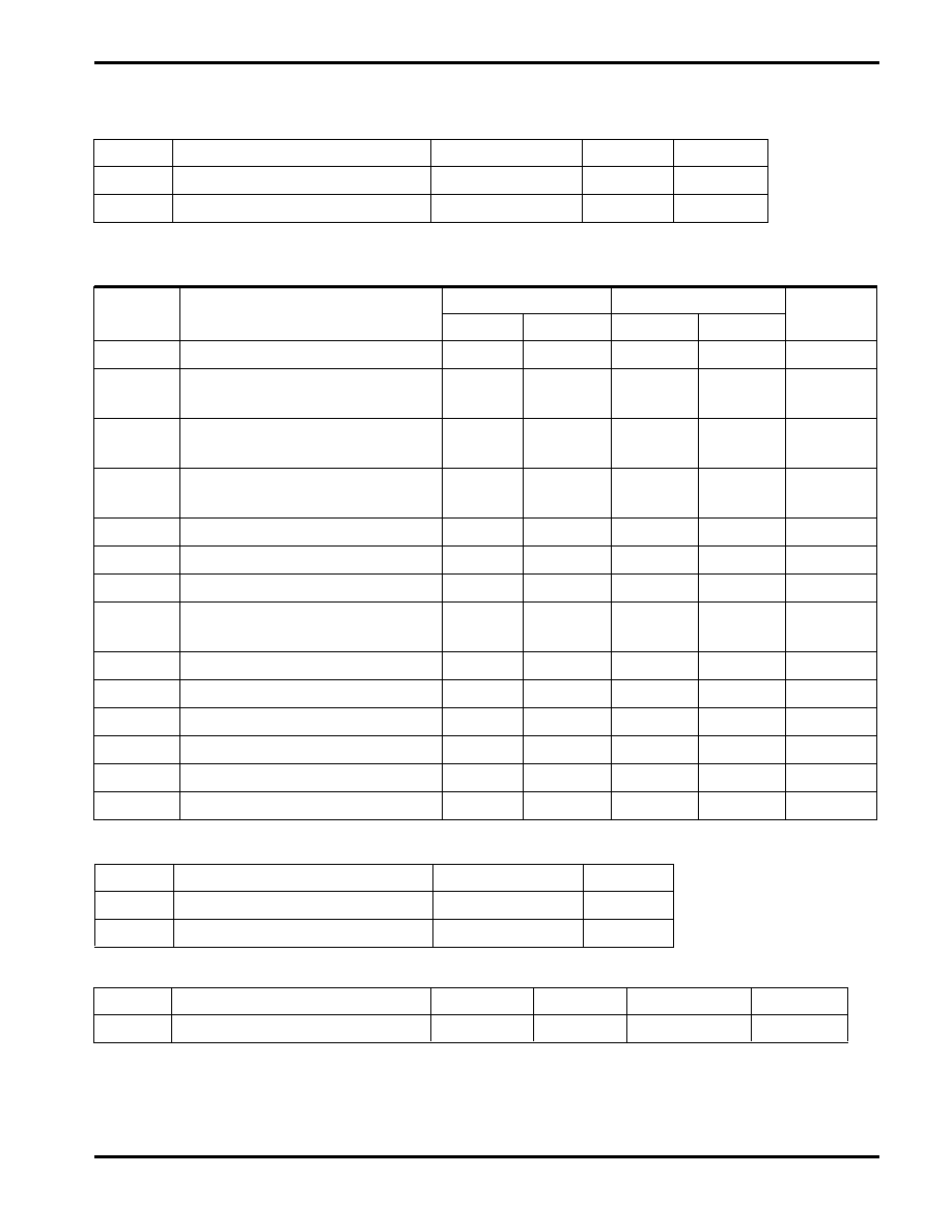
CAPACITANCE
TA = 25C, f = 1.0 MHz, VCC = 5V
Symbol
Test
Conditions
Max
Units
CI/O(1)
Input/Output Capacitance (SDA)
VI/O = 0V
8
pF
CIN(1)
Input Capacitance (SCL)
VIN = 0V
6
pF
VCC = 2.7V - 6V
VCC = 4.5V - 5.5V
SYMBOL
PARAMETER
Min
Max
Min
Max
Units
FSCL
Clock Frequency
100
400
kHz
TI(1)
Noise Suppresion Time
200
ns
Constant at SCL, SDA Inputs
tAA
SLC Low to SDA Data Out
3.5
1
s
and ACK Out
tBUF(1)
Time the Bus Must be Free Before
4.7
1.2
s
a New Transmission Can Start
tHD:STA
Start Condition Hold Time
4
0.6
s
tLOW
Clock Low Period
4.7
1.2
s
tHIGH
Clock High Period
4
0.6
s
tSU:STA
Start Condition Setup Time
4.7
0.6
s
(for a Repeated Start Condition)
tHD:DAT
Data in Hold Time
0
ns
tSU:DAT
Data in Setup Time
50
ns
tR(1)
SDA and SCL Rise Time
1
0.3
s
tF(1)
SDA and SCL Fall Time
300
ns
tSU:STO
Stop Condition Setup Time
4
0.6
s
tDH
Data Out Hold Time
100
ns
A.C. CHARACTERISTICS
VCC=2.7V to 6.0V unless otherwise specified.
Output Load is 1 TTL Gate and 100pF.
POWER-UP TIMING (1)(2)
Symbol
Parameter
Max
Units
tPUR
Power-up to Read Operation
1
ms
tPUW
Power-up to Write Operation
1
ms
NOTE:
(1) This parameter is tested initially and after a design or process change that affects the parameter.
(2) tPUR and tPUW are the delays required from the time VCC is stable until the specific operation can be initiated.
WRITE CYCLE LIMITS
Symbol
Parameter
Min
Typ
Max
Units
tWR
Write Cycle Time
10
ms
The write cycle time is the time from a valid stop condition of a write sequence to the end of the internal program/erase cycle. During the
write cycle, the bus interface circuits are disabled, SDA is allowed to remain high, and the device does not respond to its slave address.
相关PDF资料 |
PDF描述 |
|---|---|
| CAT1162J-25 | I2C Serial EEPROM with Supervisory Features |
| CAT1162J-28 | 1.25A SCRS |
| CAT1162WI-25-GT3 | 1-CHANNEL POWER SUPPLY SUPPORT CKT, PDSO8 |
| CAT1162WI-28-GT3 | 1-CHANNEL POWER SUPPLY SUPPORT CKT, PDSO8 |
| CAT22C10JA-30 | 64 X 4 NON-VOLATILE SRAM, 300 ns, PDSO16 |
相关代理商/技术参数 |
参数描述 |
|---|---|
| CAT1161W28 | 制造商:ON Semiconductor 功能描述: |
| CAT1161W-28 | 制造商:ON Semiconductor 功能描述:SUPERVISORY CCT 16K E2 SMD 1161 |
| CAT1161W-28 | 制造商:ON Semiconductor 功能描述:IC SM SUPERVISORY CCT W/ 16K E2 |
| CAT1161W-30 | 制造商:ON Semiconductor 功能描述:SUPERVISORY CCT 16K E2 SMD 1161 |
| CAT1161W-30 | 制造商:ON Semiconductor 功能描述:IC SM SUPERVISORY CCT W/ 16K E2 |
发布紧急采购,3分钟左右您将得到回复。