- 您现在的位置:买卖IC网 > PDF目录169495 > CAT25040UE-1.8REV-C (ON SEMICONDUCTOR) 512 X 8 SPI BUS SERIAL EEPROM, PDSO8 PDF资料下载
参数资料
| 型号: | CAT25040UE-1.8REV-C |
| 厂商: | ON SEMICONDUCTOR |
| 元件分类: | PROM |
| 英文描述: | 512 X 8 SPI BUS SERIAL EEPROM, PDSO8 |
| 封装: | TSSOP-8 |
| 文件页数: | 10/11页 |
| 文件大小: | 114K |
| 代理商: | CAT25040UE-1.8REV-C |
8
CAT25010/20/40
Doc. No. 1006, Rev. M
2005 by Catalyst Semiconductor, Inc.
Characteristics subject to change without notice
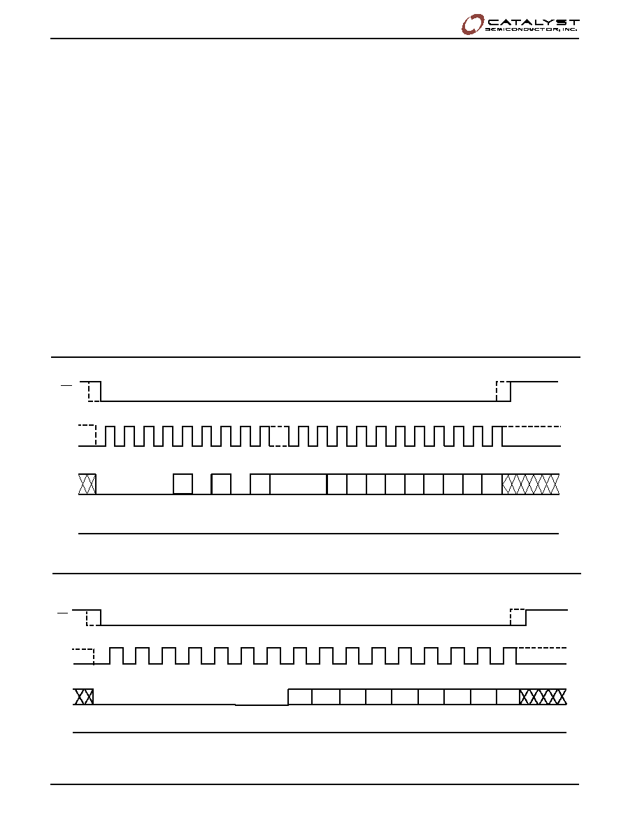
Figure 7. WRSR Timing
Figure 6. Write Instruction Timing
array because the write enable latch will not have been
properly set. Also, for a successful write operation the
address of the memory location(s) to be programmed
must be outside the protected address field location
selected by the block protection level.
Byte Write
Once the device is in a Write Enable state, the user may
proceed with a write sequence by setting the
CS low,
issuing a write instruction via the SI line, followed by the
8-bit address for 25010/20/40 (for the 25040, bit 3 of the
read data instruction contains address A8). Programming
will start after the
CS is brought high. Figure 6 illustrates
byte write sequence.
During an internal write cycle, all commands will be
ignored except the RDSR (Read Status Register)
instruction.
The Status Register can be read to determine if the write
cycle is still in progress. If Bit 0 of the Status Register is
set at 1, write cycle is in progress. If Bit 0 is set at 0, the
Note: Dashed Line= mode (1, 1) – ––––
*X=0 for 25010, 25020 ; X=A8 for 25040
Note: Dashed Line= mode (1, 1) – ––––
SK
SI
SO
00
10
BYTE ADDRESS
D7 D6 D5 D4 D3 D2 D1 D0
012345678
13
14
15
16
17
18
19
20
21
22
23
CS
OPCODE
DATA IN
HIGH IMPEDANCE
X*
A7
A0
0
1
2
345
67
8
10
911
12
13
14
SCK
SI
MSB
HIGH IMPEDANCE
DATA IN
15
SO
CS
7
6
5
4
3
2
10
00
0
00
0
1
OPCODE
device is ready for the next instruction
Page Write
The CAT25010/20/40 features page write capability.
After the initial byte, the host may continue to write up to
16 bytes of data to the CAT25010/20/40. After each
byte of data received, lower order address bits are
internally incremented by one; the high order bits of
address will remain constant. The only restriction is that
the X (X=16 for CAT25010/20/40) bytes must reside on
the same page. If the address counter reaches the end
of the page and clock continues, the counter will “roll
over” to the first address of the page and overwrite any
data that may have been written. The CAT25010/20/40
is automatically returned to the write disable state at the
completion of the write cycle. Figure 8 illustrates the
page write sequence.
To write to the status register, the WRSR instruction
should be sent. Only Bit 2 and Bit 3 of the status register
can be written using the WRSR instruction. Figure 7
illustrates the sequence of writing to status register.
相关PDF资料 |
PDF描述 |
|---|---|
| CAT25040VA-REV-C | 512 X 8 SPI BUS SERIAL EEPROM, PDSO8 |
| CAT25040VE-1.8TE13REV-C | 512 X 8 SPI BUS SERIAL EEPROM, PDSO8 |
| CAT25040Z-1.8TE13REV-C | 512 X 8 SPI BUS SERIAL EEPROM, PDSO8 |
| CAT25C65V-1.8TE13 | 8K X 8 SPI BUS SERIAL EEPROM, PDSO8 |
| CAT25C65Y14I-1.8 | 8K X 8 SPI BUS SERIAL EEPROM, PDSO14 |
相关代理商/技术参数 |
参数描述 |
|---|---|
| CAT25040UI | 功能描述:电可擦除可编程只读存储器 (512x8) 4K 2.5-6.0 RoHS:否 制造商:Atmel 存储容量:2 Kbit 组织:256 B x 8 数据保留:100 yr 最大时钟频率:1000 KHz 最大工作电流:6 uA 工作电源电压:1.7 V to 5.5 V 最大工作温度:+ 85 C 安装风格:SMD/SMT 封装 / 箱体:SOIC-8 |
| CAT25040UI-1.8 | 功能描述:电可擦除可编程只读存储器 (512x8) 4K 1.8-6.0 RoHS:否 制造商:Atmel 存储容量:2 Kbit 组织:256 B x 8 数据保留:100 yr 最大时钟频率:1000 KHz 最大工作电流:6 uA 工作电源电压:1.7 V to 5.5 V 最大工作温度:+ 85 C 安装风格:SMD/SMT 封装 / 箱体:SOIC-8 |
| CAT25040V | 功能描述:电可擦除可编程只读存储器 (512x8) 4K 2.5-6.0 RoHS:否 制造商:Atmel 存储容量:2 Kbit 组织:256 B x 8 数据保留:100 yr 最大时钟频率:1000 KHz 最大工作电流:6 uA 工作电源电压:1.7 V to 5.5 V 最大工作温度:+ 85 C 安装风格:SMD/SMT 封装 / 箱体:SOIC-8 |
| CAT25040V-1.8 | 功能描述:电可擦除可编程只读存储器 (512x8) 4K 1.8-6.0 RoHS:否 制造商:Atmel 存储容量:2 Kbit 组织:256 B x 8 数据保留:100 yr 最大时钟频率:1000 KHz 最大工作电流:6 uA 工作电源电压:1.7 V to 5.5 V 最大工作温度:+ 85 C 安装风格:SMD/SMT 封装 / 箱体:SOIC-8 |
| CAT25040VA | 功能描述:电可擦除可编程只读存储器 (512x8) 4K 2.5-6.0 RoHS:否 制造商:Atmel 存储容量:2 Kbit 组织:256 B x 8 数据保留:100 yr 最大时钟频率:1000 KHz 最大工作电流:6 uA 工作电源电压:1.7 V to 5.5 V 最大工作温度:+ 85 C 安装风格:SMD/SMT 封装 / 箱体:SOIC-8 |
发布紧急采购,3分钟左右您将得到回复。