- 您现在的位置:买卖IC网 > PDF目录20249 > CAT6218-285TDGT3 (ON Semiconductor)IC REG LDO 2.85V .3A TSOT23-5 PDF资料下载
参数资料
| 型号: | CAT6218-285TDGT3 |
| 厂商: | ON Semiconductor |
| 文件页数: | 2/9页 |
| 文件大小: | 0K |
| 描述: | IC REG LDO 2.85V .3A TSOT23-5 |
| 标准包装: | 3,000 |
| 稳压器拓扑结构: | 正,固定式 |
| 输出电压: | 2.85V |
| 输入电压: | 最高 5.5V |
| 电压 - 压降(标准): | 0.18V @ 300mA |
| 稳压器数量: | 1 |
| 电流 - 输出: | 300mA |
| 工作温度: | -40°C ~ 125°C |
| 安装类型: | 表面贴装 |
| 封装/外壳: | SOT-23-5 细型,TSOT-23-5 |
| 供应商设备封装: | TSOT-23-5 |
| 包装: | 带卷 (TR) |
�� �
�
�CAT6218�
�V� IN�
�2.3� V�
�to� 5.5� V�
�C� IN�
�1� μ� F�
�VIN� VOUT�
�CAT6218�
�V� OUT�
�C� OUT�
�1� μ� F�
�V� IN�
�VIN�
�EN�
�LDO�
�VOUT�
�V� OUT�
�OFF�
�ON�
�EN�
�BYP�
�GND�
�C� BYP� (Optional)�
�10� nF�
�BYP�
�Reference�
�Shutdown�
�Switch�
�GND�
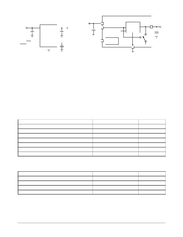
�Figure� 1.� Typical� Application� Circuit�
�Pin� Function�
�VIN� is� the� supply� pin� for� the� LDO.� A� small� 1� m� F� ceramic�
�bypass� capacitor� is� required� between� the� V� IN� pin� and� ground�
�near� the� device.� When� using� longer� connections� to� the� power�
�supply,� C� IN� value� can� be� increased� without� limit.� The�
�operating� input� voltage� range� is� from� 2.3� V� to� 5.5� V.�
�EN� is� the� enable� control� logic� (active� high)� for� the� regulator�
�output.� It� has� a� 2.5� M� W� pull� ?� down� resistor,� which� assures�
�that� if� EN� pin� is� left� open,� the� circuit� is� disabled.�
�VOUT� is� the� LDO� regulator� output.� A� small� 1� m� F� ceramic�
�bypass� capacitor� is� required� between� the� V� OUT� pin� and�
�ground� for� stability.� For� better� transient� response,� its� value�
�can� be� increased� to� 4.7� m� F.�
�Table� 1.� ABSOLUTE� MAXIMUM� RATINGS�
�Figure� 2.� CAT6218� Functional� Block� Diagram�
�The� capacitor� should� be� located� near� the� device.� ESR�
�domain� is� 5� m� W� to� 500� m� W� .� V� OUT� can� deliver� a� maximum�
�guaranteed� current� of� 300� mA.� For� input� ?� to� ?� output� voltages�
�higher� than� 1� V,� a� continuous� 300� mA� output� current� might�
�turn� ?� on� the� thermal� protection.� A� 250� W� internal� shutdown�
�switch� discharges� the� output� capacitor� in� the� no� ?� load�
�condition.�
�GND� is� the� ground� reference� for� the� LDO.� The� pin� must� be�
�connected� to� the� ground� plane� on� the� PCB.�
�BYP� is� the� reference� bypass� pin.� An� optional� 0.01� m� F�
�capacitor� can� be� connected� between� BYP� pin� and� GND� to�
�reduce� the� output� noise� and� enhance� the� PSRR� at� high�
�frequency.�
�Parameter�
�V� IN�
�V� EN� ,� V� OUT�
�Junction� Temperature,� T� J�
�Power� Dissipation,� P� D�
�Storage� Temperature� Range,� T� S�
�Lead� Temperature� (soldering,� 5� sec.)�
�ESD� Rating� (Human� Body� Model)�
�Rating�
�0� to� 6.5�
�?� 0.3� to� V� IN� +� 0.3�
�+150�
�Internally� Limited� (Note� 1)�
�?� 65� to� +150�
�260�
�3�
�Unit�
�V�
�V�
�_� C�
�mW�
�_� C�
�_� C�
�kV�
�Stresses� exceeding� Maximum� Ratings� may� damage� the� device.� Maximum� Ratings� are� stress� ratings� only.� Functional� operation� above� the�
�Recommended� Operating� Conditions� is� not� implied.� Extended� exposure� to� stresses� above� the� Recommended� Operating� Conditions� may� affect�
�device� reliability.�
�Table 2. RECOMMENDED OPERATING CONDITIONS� (Note� 2)�
�Parameter�
�V� IN�
�V� EN�
�Junction� Temperature� Range,� T� J�
�Package� Thermal� Resistance� (SOT23� ?� 5),� θ� JA�
�Range�
�2.3� to� 5.5�
�0� to� V� IN�
�?� 40� to� +125�
�235�
�Unit�
�V�
�V�
�_� C�
�_� C/W�
�NOTE:� Typical� application� circuit� with� external� components� is� shown� above.�
�1.� The� maximum� allowable� power� dissipation� at� any� T� A� (ambient� temperature)� is� P� Dmax� =� (T� Jmax� ?� T� A� )/� q� JA� .� Exceeding� the� maximum� allowable�
�power� dissipation� will� result� in� excessive� die� temperature,� and� the� regulator� will� go� into� thermal� shutdown.�
�2.� The� device� is� not� guaranteed� to� work� outside� its� operating� rating.�
�http://onsemi.com�
�2�
�相关PDF资料 |
PDF描述 |
|---|---|
| HR-4/5AUF3 | BATT PACK 3.6V 4/5A 1900MAH NIMH |
| T86C106K010ESSS | CAP TANT 10UF 10V 10% 2312 |
| V375B48C300BG3 | CONVERTER MOD DC/DC 48V 300W |
| T86C226M6R3ESSS | CAP TANT 22UF 6.3V 20% 2312 |
| CAT6218-180TDGT3 | IC REG LDO 1.8V .3A TSOT-23-5 |
相关代理商/技术参数 |
参数描述 |
|---|---|
| CAT6218-285TD-GT3 | 制造商:CATALYST 制造商全称:Catalyst Semiconductor 功能描述:300mA CMOS LDO Regulator |
| CAT6218-300TDGT3 | 功能描述:低压差稳压器 - LDO LDO 300mA RoHS:否 制造商:Texas Instruments 最大输入电压:36 V 输出电压:1.4 V to 20.5 V 回动电压(最大值):307 mV 输出电流:1 A 负载调节:0.3 % 输出端数量: 输出类型:Fixed 最大工作温度:+ 125 C 安装风格:SMD/SMT 封装 / 箱体:VQFN-20 |
| CAT6218-300TD-GT3 | 制造商:CATALYST 制造商全称:Catalyst Semiconductor 功能描述:300mA CMOS LDO Regulator |
| CAT6218-320TDGT3 | 功能描述:低压差稳压器 - LDO 300mA 3.2 Volt RoHS:否 制造商:Texas Instruments 最大输入电压:36 V 输出电压:1.4 V to 20.5 V 回动电压(最大值):307 mV 输出电流:1 A 负载调节:0.3 % 输出端数量: 输出类型:Fixed 最大工作温度:+ 125 C 安装风格:SMD/SMT 封装 / 箱体:VQFN-20 |
| CAT6218-320TD-GT3 | 制造商:CATALYST 制造商全称:Catalyst Semiconductor 功能描述:300mA CMOS LDO Regulator |
发布紧急采购,3分钟左右您将得到回复。