参数资料
| 型号: | CAT93C57LI-G |
| 厂商: | ON Semiconductor |
| 文件页数: | 5/17页 |
| 文件大小: | 0K |
| 描述: | IC EEPROM 2KBIT 2MHZ 8DIP |
| 标准包装: | 50 |
| 格式 - 存储器: | EEPROMs - 串行 |
| 存储器类型: | EEPROM |
| 存储容量: | 2K(256 x 8 或 128 x 16) |
| 速度: | 2MHz |
| 接口: | Microwire 3 线串行 |
| 电源电压: | 1.8 V ~ 5.5 V |
| 工作温度: | -40°C ~ 85°C |
| 封装/外壳: | 8-DIP(0.300",7.62mm) |
| 供应商设备封装: | 8-PDIP |
| 包装: | 管件 |
| 其它名称: | CAT93C57LI-G-ND CAT93C57LI-GOS |
�� �
�
�CAT93C56,� CAT93C57�
�Table� 9.� A.C.� TEST� CONDITIONS�
�Input� Rise� and� Fall� Times�
�≤� 50� ns�
�Input� Pulse� Voltages�
�Timing� Reference� Voltages�
�Input� Pulse� Voltages�
�Timing� Reference� Voltages�
�0.4� V� to� 2.4� V�
�0.8� V,� 2.0� V�
�0.2� V� CC� to� 0.7� V� CC�
�0.5� V� CC�
�4.5� V� v� V� CC� v� 5.5� V�
�4.5� V� v� V� CC� v� 5.5� V�
�1.8� V� v� V� CC� v� 4.5� V�
�1.8� V� v� V� CC� v� 4.5� V�
�Output� Load�
�Device� Operation�
�The� CAT93C56/57� is� a� 2048� ?� bit� nonvolatile� memory�
�intended� for� use� with� industry� standard� microprocessors.�
�The� CAT93C56/57� can� be� organized� as� either� registers� of� 16�
�bits� or� 8� bits.� When� organized� as� X16,� seven� 10� ?� bit�
�instructions� for� 93C57� or� seven� 11� ?� bit� instructions� for�
�93C56� control� the� reading,� writing� and� erase� operations� of�
�the� device.� When� organized� as� X8,� seven� 11� ?� bit� instructions�
�for� 93C57� or� seven� 12� ?� bit� instructions� for� 93C56� control� the�
�reading,� writing� and� erase� operations� of� the� device.� The�
�CAT93C56/57� operates� on� a� single� power� supply� and� will�
�generate� on� chip,� the� high� voltage� required� during� any� write�
�operation.�
�Instructions,� addresses,� and� write� data� are� clocked� into� the�
�DI� pin� on� the� rising� edge� of� the� clock� (SK).� The� DO� pin� is�
�normally� in� a� high� impedance� state� except� when� reading� data�
�Current� Source� I� OLmax� /I� OHmax� ;� CL=100� pF�
�from� the� device,� or� when� checking� the� ready/busy� status�
�after� a� write� operation.� The� serial� communication� protocol�
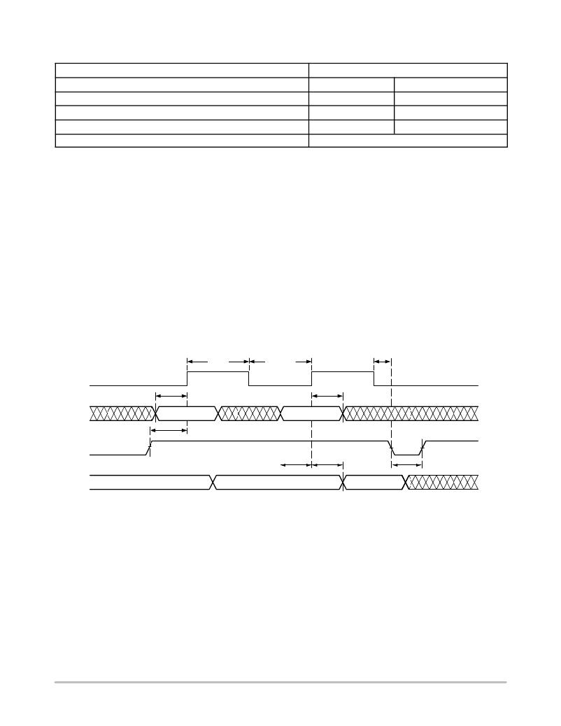
�follows� the� timing� shown� in� Figure� 2.�
�The� ready/busy� status� can� be� determined� after� the� start� of�
�internal� write� cycle� by� selecting� the� device� (CS� high)� and�
�polling� the� DO� pin;� DO� low� indicates� that� the� write�
�operation� is� not� completed,� while� DO� high� indicates� that� the�
�device� is� ready� for� the� next� instruction.� If� necessary,� the� DO�
�pin� may� be� placed� back� into� a� high� impedance� state� during�
�chip� select� by� shifting� a� dummy� “1”� into� the� DI� pin.� The� DO�
�pin� will� enter� the� high� impedance� state� on� the� rising� edge� of�
�the� clock� (SK).� Placing� the� DO� pin� into� the� high� impedance�
�state� is� recommended� in� applications� where� the� DI� pin� and�
�the� DO� pin� are� to� be� tied� together� to� form� a� common� DI/O�
�pin.�
�SK�
�t� DIS�
�t� SKHI�
�t� SKLOW�
�t� DIH�
�t� CSH�
�DI�
�CS�
�t� CSS�
�V� ALID�
�VALID�
�DO�
�t� DIS�
�t� PD0� ,� t� PD1�
�DATA� VALID�
�t� CSMN�
�Figure� 2.� Synchronous� Data� Timing�
�http://onsemi.com�
�5�
�相关PDF资料 |
PDF描述 |
|---|---|
| M7A3P1000-FGG256I | IC FPGA 1KB FLASH 1M 256-FBGA |
| M7A3P1000-FG256I | IC FPGA 1KB FLASH 1M 256-FBGA |
| A54SX16P-1TQ144 | IC FPGA SX 24K GATES 144-TQFP |
| A1010B-2VQ80C | IC FPGA 1200 GATES 80-VQFP COM |
| A1010B-2VQG80C | IC FPGA 1200 GATES 80-VQFP COM |
相关代理商/技术参数 |
参数描述 |
|---|---|
| CAT93C57LI-GT2 | 制造商:ONSEMI 制造商全称:ON Semiconductor 功能描述:2-Kb Microwire Serial CMOS EEPROM |
| CAT93C57LI-GT2E | 制造商:ONSEMI 制造商全称:ON Semiconductor 功能描述:2-Kb Microwire Serial CMOS EEPROM |
| CAT93C57LI-GT3 | 制造商:ONSEMI 制造商全称:ON Semiconductor 功能描述:2-Kb Microwire Serial CMOS EEPROM |
| CAT93C57LI-GT3E | 制造商:ONSEMI 制造商全称:ON Semiconductor 功能描述:2-Kb Microwire Serial CMOS EEPROM |
| CAT93C57LIT2 | 制造商:ONSEMI 制造商全称:ON Semiconductor 功能描述:2-Kb Microwire Serial CMOS EEPROM |
发布紧急采购,3分钟左右您将得到回复。