- 您现在的位置:买卖IC网 > PDF目录67391 > CBT3306GM (NXP SEMICONDUCTORS) Dual bus switch PDF资料下载
参数资料
| 型号: | CBT3306GM |
| 厂商: | NXP SEMICONDUCTORS |
| 元件分类: | 总线收发器 |
| 英文描述: | Dual bus switch |
| 中文描述: | CBT/FST/QS/5C/B SERIES, DUAL 1-BIT DRIVER, TRUE OUTPUT, PQCC8 |
| 封装: | 1.6 X1.6 MM, 0.5 MM HEIGHT, PLASTIC, MO-255, SOT-902-1, XQFN-8 |
| 文件页数: | 9/14页 |
| 文件大小: | 250K |
| 代理商: | CBT3306GM |
CBT3306_5
NXP B.V. 2010. All rights reserved.
Product data sheet
Rev. 05 — 25 March 2010
4 of 14
NXP Semiconductors
CBT3306
Dual bus switch
10. Static characteristics
[1]
All typical values are at VCC = 5 V, Tamb = 25 °C.
[2]
This is the increase in supply current for each input that is at the specified TTL voltage level rather than VCC or GND.
[3]
Measured by the voltage drop between the nA and the nB terminals at the indicated current through the switch. ON resistance is
determined by the lowest voltage of the two (nA, nB) terminals.
11. Dynamic characteristics
[1]
The propagation delay is the calculated RC time constant of the typical ON resistance of the switch and the specified load capacitance,
when driven by an ideal voltage source (zero output impedance).
[2]
tpd is the same as tPLH and tPHL.
ten is the same as tPZL and tPZH.
tdis is the same as tPLZ and tPHZ.
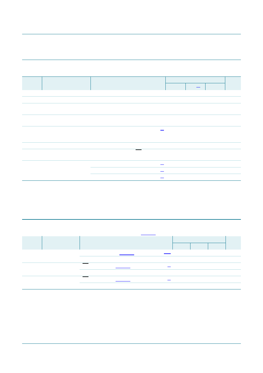
Table 7.
Static characteristics
Voltages are referenced to GND (ground = 0 V).
Symbol
Parameter
Conditions
40 °C to +85 °C
Unit
Min
Typ[1]
Max
VIK
input clamping voltage
VCC = 4.5 V; II = 18 mA
-
1.2
V
II
input leakage current
VCC = 5.5 V; VI = GND or 5.5 V
-
±1
μA
ICC
supply current
VCC = 5.5 V; IO = 0 mA;
VI = VCC or GND
-
3
μA
Vpass
pass voltage
output HIGH; VI = VCC = 5.0 V;
IO = 100 μA
3.6
3.9
4.2
V
ΔI
CC
additional supply current
per input pin; VCC = 5.5 V;
one input at 3.4 V, other inputs at
VCC or GND
-
2.5
mA
CI
input capacitance
control pin; VI = 3 V or 0 V
-
3.15
-
pF
Cio(off)
off-state input/output
capacitance
port off; VI = 3 V or 0 V; nOE = VCC
-
6.45
-
pF
RON
ON resistance
VCC = 4.5 V; VI = 0 V; II = 64 mA
-
3.4
5
Ω
VCC = 4.5 V; VI = 0 V; II = 30 mA
-
3.4
5
Ω
VCC = 4.5 V; VI = 2.4 V; II = 15 mA
-
6.8
15
Ω
Table 8.
Dynamic characteristics
Voltages are referenced to GND (ground = 0 V). For test circuit see Figure 8.
Symbol
Parameter
Conditions
40 °C to +85 °C
Unit
Min
Typ
Max
tpd
propagation delay
nA, nB to nB, nA; see Figure 6
-
0.25
ns
VCC = 5.0 V ± 0.5 V
ten
enable time
nOE to nA, nB; see Figure 7
1.0
-
5.0
ns
VCC = 5.0 V ± 0.5 V
tdis
disable time
nOE to nA, nB; see Figure 7
1.0
-
5.0
ns
VCC = 5.0 V ± 0.5 V
相关PDF资料 |
PDF描述 |
|---|---|
| CBT3306PW | Dual bus switch |
| CBT3384DB | 10-bit bus switch with 5-bit output enables |
| CBT3384D | 10-bit bus switch with 5-bit output enables |
| CBT3384PW | 10-bit bus switch with 5-bit output enables |
| CBT3384DK | 10-bit bus switch with 5-bit output enables |
相关代理商/技术参数 |
参数描述 |
|---|---|
| CBT3306GM,125 | 功能描述:数字总线开关 IC DUAL BUS SWITCH RoHS:否 制造商:Texas Instruments 开关数量:24 传播延迟时间:0.25 ns 最大工作温度:+ 85 C 最小工作温度:- 40 C 封装 / 箱体:TSSOP-56 封装:Reel |
| CBT3306GT | 制造商:NXP Semiconductors 功能描述:Cut Tape |
| CBT3306GT,115 | 功能描述:数字总线开关 IC Dual 15Ohms 5.5V RoHS:否 制造商:Texas Instruments 开关数量:24 传播延迟时间:0.25 ns 最大工作温度:+ 85 C 最小工作温度:- 40 C 封装 / 箱体:TSSOP-56 封装:Reel |
| CBT3306PW | 制造商:PHILIPS 制造商全称:NXP Semiconductors 功能描述:Dual bus switch |
| CBT3306PW,118 | 功能描述:数字总线开关 IC DUAL BUS SWITCH RoHS:否 制造商:Texas Instruments 开关数量:24 传播延迟时间:0.25 ns 最大工作温度:+ 85 C 最小工作温度:- 40 C 封装 / 箱体:TSSOP-56 封装:Reel |
发布紧急采购,3分钟左右您将得到回复。