- 您现在的位置:买卖IC网 > PDF目录373036 > CBTD16211DGG 24-bit level shifting bus exchange switch with 12-bit output enables PDF资料下载
参数资料
| 型号: | CBTD16211DGG |
| 英文描述: | 24-bit level shifting bus exchange switch with 12-bit output enables |
| 中文描述: | 24位电平转换与12位输出使能的总线交换开关 |
| 文件页数: | 4/10页 |
| 文件大小: | 77K |
| 代理商: | CBTD16211DGG |
Philips Semiconductors
Product data
CBTD16211
24-bit level shifting bus exchange switch
with 12-bit output enables
2001 Jun 13
4
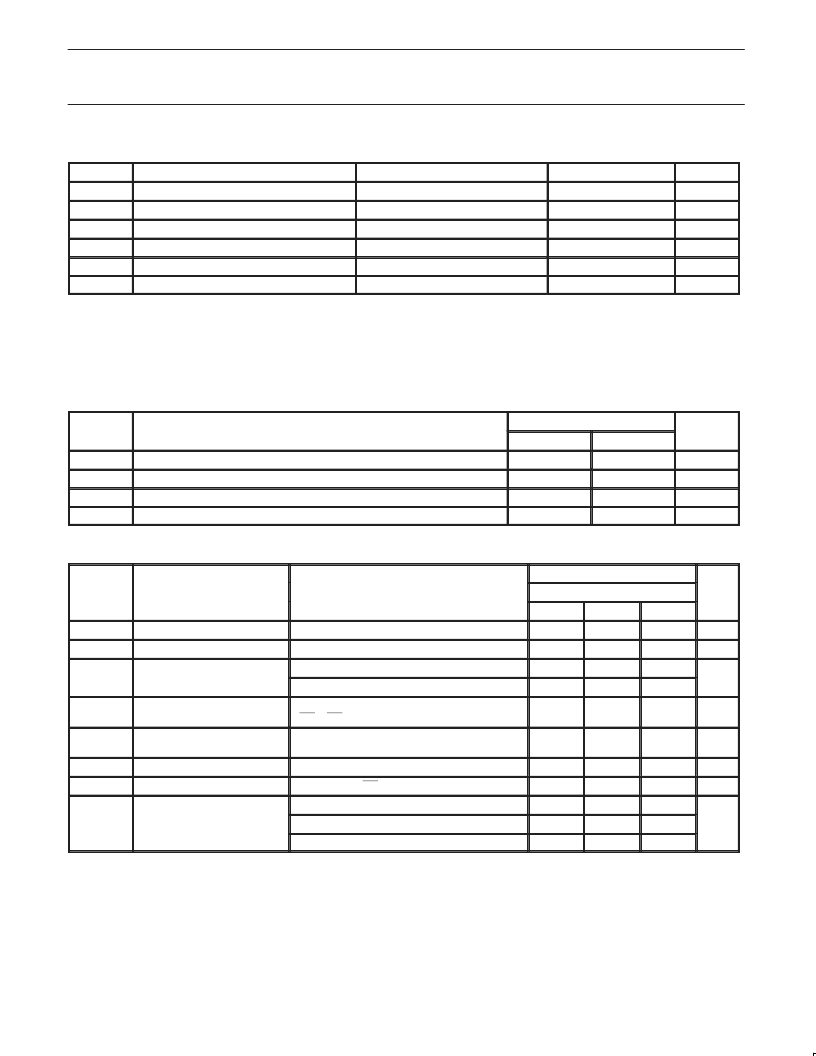
ABSOLUTE MAXIMUM RATINGS
1, 2
SYMBOL
PARAMETER
CONDITIONS
RATING
UNIT
V
CC
I
IK
V
I
V
OUT
I
OUT
T
stg
DC supply voltage
–0.5 to +7.0
V
DC input diode current
DC input voltage
3
DC output voltage
3
V
I
< 0
–50
mA
–0.5 to +7.0
V
output in Off or High state
–0.5 to +5.5
V
DC output current
output in Low state
128
mA
Storage temperature range
–65 to +150
°
C
NOTES:
1. Stresses beyond those listed may cause permanent damage to the device. These are stress ratings only and functional operation of the
device at these or any other conditions beyond those indicated under “recommended operating conditions” is not implied. Exposure to
absolute-maximum-rated conditions for extended periods may affect device reliability.
2. The performance capability of a high-performance integrated circuit in conjunction with its thermal environment can create junction
temperatures which are detrimental to reliability. The maximum junction temperature of this integrated circuit should not exceed 150
°
C.
3. The input and output voltage ratings may be exceeded if the input and output current ratings are observed.
RECOMMENDED OPERATING CONDITIONS
SYMBOL
PARAMETER
LIMITS
UNIT
Min
Max
V
CC
V
IH
V
IL
T
amb
DC supply voltage
4.5
5.5
V
High-level input voltage
2.0
—
V
Low-level Input voltage
—
0.8
V
Operating free-air temperature range
–40
+85
°
C
DC ELECTRICAL CHARACTERISTICS
LIMITS
SYMBOL
PARAMETER
TEST CONDITIONS
T
amb
= –40 to +85
°
C
Min
Typ
1
UNIT
Max
V
IK
V
OH
Input clamp voltage
V
CC
= 4.5 V; I
I
= –18 mA
See Figure 1
—
—
–1.2
V
Output high pass voltage
—
—
V
I
I
Input leakage current
V
CC
= 0 V; V
I
= 5.5 V
V
CC
= 5.5 V; V
I
= GND or 5.5 V
V
CC
= 5.5 V; I
O
= 0, V
I
= V
CC
or GND;
1OE=2OE=GND
—
—
10
μ
A
—
—
±
1
I
CC
Quiescent supply current
—
—
1.5
mA
I
CC
Additional supply current per
input pin
2
V
CC
= 5.5 V, one input at 3.4 V,
other inputs at V
CC
or GND
V
I
= 3 V or 0
V
O
= 3 V or 0, OE = V
CC
V
CC
= 4.5 V; V
1
= 0 V; I
I
= 64 mA
V
CC
= 4.5 V; V
1
= 0 V; I
I
= 30 mA
V
CC
= 4.5 V; V
1
= 2.4 V; I
I
= –15 mA
—
—
2.5
mA
C
I
Control pins
—
4.5
—
pF
C
I(OFF)
Port OFF capacitance
—
8
—
pF
—
5
7
r
on3
—
5
7
—
35
50
NOTES:
1. All typical values are at V
CC
= 5 V, T
amb
= 25
°
C.
2. This is the increase in supply current for each input that is at the specified TTL voltage level rather than V
CC
or GND.
3. Measured by the voltage drop between the A and the B terminals at the indicated current through the switch.
On-state resistance is determined by the lowest voltage of the two (A or B) terminals.
相关PDF资料 |
PDF描述 |
|---|---|
| CBTD16211DL | 24-bit level shifting bus exchange switch with 12-bit output enables |
| CBTD3306 | Dual bus switch with level shifting |
| CD3016B | 1 WATT CAPABILITY WITH PROPER HEAT SINKING |
| CD3017B | 1 WATT CAPABILITY WITH PROPER HEAT SINKING |
| CD3018B | 1 WATT CAPABILITY WITH PROPER HEAT SINKING |
相关代理商/技术参数 |
参数描述 |
|---|---|
| CBTD16211DGG,112 | 功能描述:数字总线开关 IC 24BIT BUS SW W/12BIT OUTPUT EN RoHS:否 制造商:Texas Instruments 开关数量:24 传播延迟时间:0.25 ns 最大工作温度:+ 85 C 最小工作温度:- 40 C 封装 / 箱体:TSSOP-56 封装:Reel |
| CBTD16211DGG,118 | 功能描述:数字总线开关 IC 24BIT BUS SW W/12BIT RoHS:否 制造商:Texas Instruments 开关数量:24 传播延迟时间:0.25 ns 最大工作温度:+ 85 C 最小工作温度:- 40 C 封装 / 箱体:TSSOP-56 封装:Reel |
| CBTD16211DGG-T | 功能描述:数字总线开关 IC 24BIT BUS SW W/12BIT OUTPUT EN RoHS:否 制造商:Texas Instruments 开关数量:24 传播延迟时间:0.25 ns 最大工作温度:+ 85 C 最小工作温度:- 40 C 封装 / 箱体:TSSOP-56 封装:Reel |
| CBTD16211DL | 功能描述:数字总线开关 IC 24BIT BUS SW W/12BIT OUTPUT EN RoHS:否 制造商:Texas Instruments 开关数量:24 传播延迟时间:0.25 ns 最大工作温度:+ 85 C 最小工作温度:- 40 C 封装 / 箱体:TSSOP-56 封装:Reel |
| CBTD16211DL,512 | 功能描述:数字总线开关 IC 24BIT BUS SW W/12BIT RoHS:否 制造商:Texas Instruments 开关数量:24 传播延迟时间:0.25 ns 最大工作温度:+ 85 C 最小工作温度:- 40 C 封装 / 箱体:TSSOP-56 封装:Reel |
发布紧急采购,3分钟左右您将得到回复。