- 您现在的位置:买卖IC网 > PDF目录366832 > CD4023CJ Triple 3-input NAND Gate PDF资料下载
参数资料
| 型号: | CD4023CJ |
| 英文描述: | Triple 3-input NAND Gate |
| 中文描述: | 三3输入与非门 |
| 文件页数: | 4/9页 |
| 文件大小: | 99K |
| 代理商: | CD4023CJ |
www.fairchildsemi.com
4
C
Absolute Maximum Ratings
(Note 1)
(Note 2)
Recommended Operating
Conditions
Note 1:
“
Absolute Maximum Ratings
”
are those values beyond which the
safety of the device cannot be guaranteed. They are not meant to imply
that the devices should be operated at these limits. The tables of
“
Recom-
mended Operating Conditions
”
and
“
Electrical Characteristics
”
provide con-
ditions for actual device operation.
Note 2:
V
SS
=
0V unless otherwise specified.
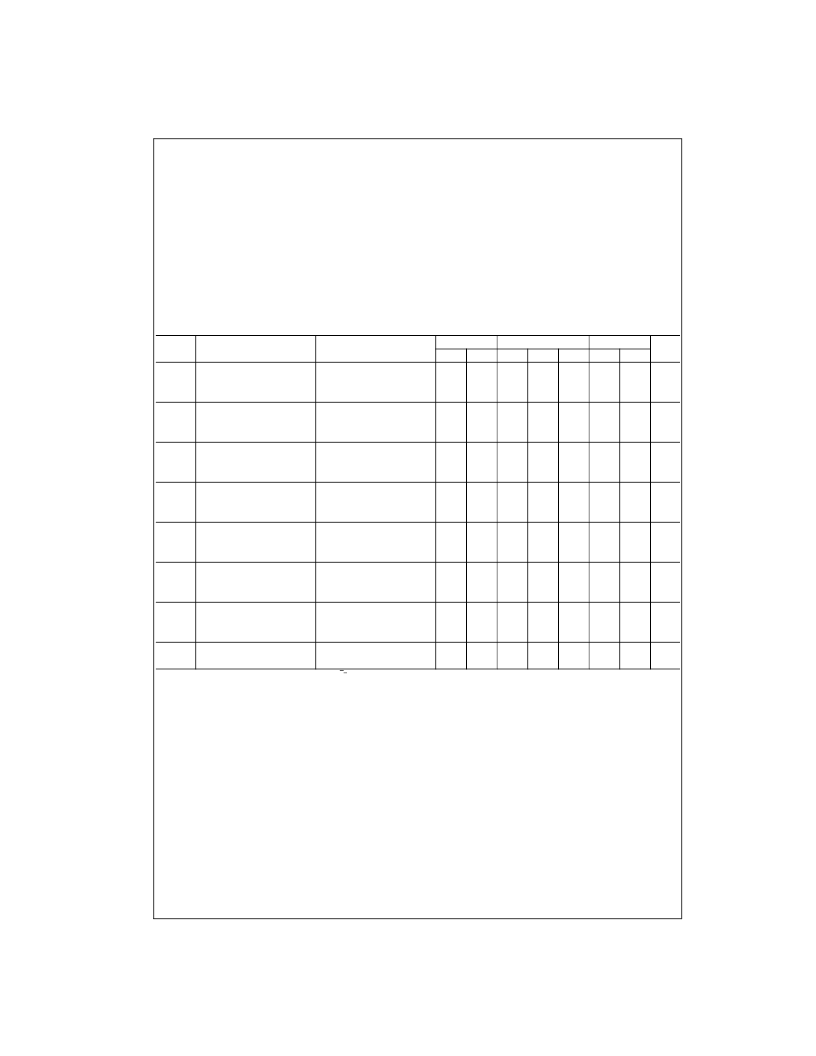
DC Electrical Characteristics
(Note 2)
Note 3:
Data does not apply to oscillator points
φ
0
and
φ
0
of CD4060BC. I
OH
and I
OL
are tested one output at a time.
Supply Voltage (V
DD
)
Input Voltage (V
IN
)
Storage Temperature Range (T
S
)
Package Dissipation (P
D
)
Dual-In-Line
Small Outline
Lead Temperature (T
L
)
(Soldering, 10 seconds)
0.5V to
+
18V
0.5V to V
DD
+
0.5V
65
°
C to
+
150
°
C
700 mW
500 mW
260
°
C
Supply Voltage (V
DD
)
Input Voltage (V
IN
)
Operating Temperature Range (T
A
)
+
3V to
+
15V
0V to V
DD
55
°
C to
+
125
°
C
Symbol
Parameter
Conditions
55
°
C
Min
+
25
°
C
Typ
+
125
°
C
Min
Units
Max
5
10
Min
Max
5
10
Max
150
300
I
DD
Quiescent Device Current
V
DD
=
5V, V
IN
=
V
DD
or V
SS
V
DD
=
10V, V
IN
=
V
DD
or V
SS
V
DD
=
15V, V
IN
=
V
DD
or V
SS
V
DD
=
5V
V
DD
=
10V
V
DD
=
15V
V
DD
=
5V
V
DD
=
10V
V
DD
=
15V
V
DD
=
5V, V
O
=
0.5V or 4.5V
V
DD
=
10V, V
O
=
1.0V or 9.0V
V
DD
=
15V, V
O
=
1.5V or 13.5V
V
DD
=
5V, V
O
=
0.5V or 4.5V
V
DD
=
10V, V
O
=
1.0V or 9.0V
V
DD
=
15V, V
O
=
1.5V or 13.5V
V
DD
=
5V, V
O
=
0.4V
V
DD
=
10V, V
O
=
0.5V
V
DD
=
15V, V
O
=
1.5V
V
DD
=
5V, V
O
=
4.6V
V
DD
=
10V, V
O
=
9.5V
V
DD
=
15V, V
O
=
13.5V
V
DD
=
15V, V
IN
=
0V
V
DD
=
15V, V
IN
=
15V
μ
A
20
0.05
0.05
20
0.05
0.05
600
0.05
0.05
V
OL
LOW Level Output Voltage
0
0
V
0.05
0
5
0.05
0.05
V
OH
HIGH Level Output Voltage
4.95
9.95
4.95
9.95
4.95
9.95
V
10
14.95
14.95
15
2
4
14.95
V
IL
LOW Level Input Voltage
1.5
3.0
1.5
3.0
1.5
3.0
V
4.0
6
3
6
4.0
4.0
V
IH
HIGH Level Input Voltage
3.5
7.0
3.5
7.0
3.5
7.0
V
11.0
0.64
1.6
11.0
0.51
1.3
9
11.0
0.36
0.9
I
OL
LOW Level Output Current
(Note 3)
0.88
2.25
mA
4.2
0.64
1.6
4.2
3.4
0.51
1.3
3.4
8.8
0.88
2.25
8.8
10
5
10
5
2.4
0.36
0.9
2.4
I
OH
HIGH Level Output Current
(Note 3)
mA
I
IN
Input Current
0.1
0.1
0.1
0.1
1.0
1.0
μ
A
相关PDF资料 |
PDF描述 |
|---|---|
| CD4023CN | Triple 3-input NAND Gate |
| CD4023MD | Triple 3-input NAND Gate |
| CD4023MF | Triple 3-input NAND Gate |
| CD4023MJ | Triple 3-input NAND Gate |
| CD4023MW | Triple 3-input NAND Gate |
相关代理商/技术参数 |
参数描述 |
|---|---|
| CD4023MJ | 制造商:undefined 功能描述: |
| CD4023UBE | 制造商:RCA 功能描述: |
| CD4023UBF | 制造商:RCA 功能描述: |
| CD4024 WAF | 制造商:Fairchild Semiconductor Corporation 功能描述: |
| CD4024AD | 制造商:Rochester Electronics LLC 功能描述:- Bulk |
发布紧急采购,3分钟左右您将得到回复。