参数资料
| 型号: | CDP68HC68T1MZ |
| 厂商: | Intersil |
| 文件页数: | 6/23页 |
| 文件大小: | 0K |
| 描述: | IC RTC RAM/SPI SERIAL 20-SOIC |
| 标准包装: | 38 |
| 类型: | 时钟/日历 |
| 特点: | 警报器,闰年,方波输出,监视计时器 |
| 存储容量: | 32B |
| 时间格式: | HH:MM:SS(12/24 小时) |
| 数据格式: | YY-MM-DD-dd |
| 接口: | SPI |
| 电源电压: | 3 V ~ 6 V |
| 电压 - 电源,电池: | 2.2 V ~ 6 V |
| 工作温度: | -40°C ~ 85°C |
| 安装类型: | 表面贴装 |
| 封装/外壳: | 20-SOIC(0.295",7.50mm 宽) |
| 供应商设备封装: | 20-SOIC W |
| 包装: | 管件 |
14
FN1547.8
October 29, 2007
Functional Description
The Serial Peripheral Interface (SPI) utilized by the
CDP68HC68T1 is a serial synchronous bus for address and
data transfers. The clock, which is generated by the
microcomputer is active only during address and data
transfers. In systems using the CDP68HC05C4 or
CDP68HC05D2, the inactive clock polarity is determined by
the CPOL bit in the microcomputer’s Control Register. A
unique feature of the CDP68HC68T1 is that it automatically
determines the level of the inactive clock by sampling SCK
when CE becomes active (see Figure 8). Input data (MOSI)
is latched internally on the internal strobe edge and output
data (MISO) is shifted out on the shift edge, as defined by
Figure 8. There is one clock for each data bit transferred
(address, as well as data bits are transferred in groups of 8).
Address and Data Format
There are three types of serial transfer:
1. Address Control - Figure 9.
2. READ or WRITE Data - Figure 10.
3. Watchdog Reset (actually a non-transfer) Figure 11.
The Address/Control and Data bytes are shifted MSB first,
Into the serial data input (MOSI) and out of the serial data
output (MISO).
Any transfer of data requires an Address/Control byte to
specify a Write or Read operation and to select a Clock or
RAM location, followed by one or more bytes of data.
Data is transferred out of MISO for a Read and into MOSI for
a Write operation.
Address/Control Byte - (see Figure 9)
It is always the first byte received after CE goes true. To
transmit a new address, CE must first go false and then true
again. Bit 5 is used to select between Clock and RAM
locations.
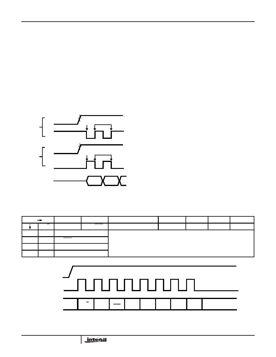
SHIFT
INTERNAL
STROBE
INTERNAL
STROBE
SHIFT
CE
SCK
CPOL = 1
SCK
CE
CPOL = 0
MOSI
MSB
MSB -1
NOTE: “CPOL” is a bit that is set in the microcomputer’s Control
Register.
FIGURE 8. SERIAL RAM CLOCK (SCK) AS A FUNCTION OF
MCU CLOCK POLARITY (CPOL)
BIT
7
6
5
4
3
2
1
0
W/R
0
CLK RAM
A4
A3
A2
A1
A0
04
A0 through A4
Selects 5-bit HEX Address of RAM or specifies Clock Register. Most Significant Address
Bit. If equal to “1”, A0 through A4 selects a Clock Register. If equal to “0”, A0 through A4
selects one of 32 RAM locations. Must be set to ”0” when not in Test Mode 7W/R W/R = “1”
initiates one or more WRITE cycles.W/R = “0”, initiates one or more READ cycles.
5CLK RAM
60
7W/R
NOTE: SCK can be either polarity.
FIGURE 9. ADDRESS/CONTROL BYTE-TRANSFER WAVEFORMS
A2
A1
A0
A3
A4
CLOCK
0
W/R
MOSI
RAM
SCK (NOTE)
CE
CDP68HC68T1
相关PDF资料 |
PDF描述 |
|---|---|
| ISL12020MIRZ | IC RTC/CALENDAR TEMP SNSR 20-DFN |
| ISL12025IBZ | IC RTC/CALENDAR EEPROM 8-SOIC |
| ISL12027AIB27Z | IC RTC/CALENDAR EEPROM 8SOIC |
| VI-JWN-MZ | CONVERTER MOD DC/DC 18.5V 25W |
| ISL12028AIB27Z | IC RTC/CALENDAR EEPROM 14SOIC |
相关代理商/技术参数 |
参数描述 |
|---|---|
| CDP68HC68T1MZ96 | 功能描述:实时时钟 W/ANEAL PERIPH SPIAL -TIME-CLK 20W IND RoHS:否 制造商:Microchip Technology 功能:Clock, Calendar. Alarm RTC 总线接口:I2C 日期格式:DW:DM:M:Y 时间格式:HH:MM:SS RTC 存储容量:64 B 电源电压-最大:5.5 V 电源电压-最小:1.8 V 最大工作温度:+ 85 C 最小工作温度: 安装风格:Through Hole 封装 / 箱体:PDIP-8 封装:Tube |
| CDP68HC68T1W | 制造商:INTERSIL 制造商全称:Intersil Corporation 功能描述:CMOS Serial Real-Time Clock With RAM and Power Sense/Control |
| CDP68HC68T1W WAF | 制造商:Harris Corporation 功能描述: |
| CDP68HC68T2D | 制造商:未知厂家 制造商全称:未知厂家 功能描述:Real-Time Clock |
| CDP68HC68T2E | 制造商:未知厂家 制造商全称:未知厂家 功能描述:Real-Time Clock |
发布紧急采购,3分钟左右您将得到回复。