- 您现在的位置:买卖IC网 > PDF目录366865 > CGA-0116 3-Output Active Splitter for CATV PDF资料下载
参数资料
| 型号: | CGA-0116 |
| 英文描述: | 3-Output Active Splitter for CATV |
| 中文描述: | 3输出有源分配器的有线电视 |
| 文件页数: | 2/8页 |
| 文件大小: | 173K |
| 代理商: | CGA-0116 |
303 South Technology Court, Broomfield, CO 80021
Phone: (800) SMI-MMIC
2
http://www.sirenza.com
EDS-102750 Rev E
Preliminary
CGA-0116 3-Output CAT V Ac tive S plitter
Pin Out Description
Pin #
Function
Description
1
Vctl 3
Gain adjust for Output 3. This pin should be bypassed to ground for max gain
2,7,10
11,14,
15
GND
Connection to ground.
3
Vin
Voltage supply connection for input. This pin should be bypassed with a suitable capacitor.
4
Vb
Bias connection for input. This pin should be bypassed with a suitable capacitor
5
IN
RF input pin. This pin requires a DC blocking capacitor
6
Rb
Input bias resistor connection for setting bias current. This pin should be connected to groung for specified
operation.
8
Vctl 1
Gain adjust for Output 3. This pin should be bypassed to ground for max gain
9
Ch. 1
RF Output 1 and DC supply pin. This pin required the use of an external blocking capacitor and RF choke.
12
Ch. 2
RF Output 2 and DC supply pin. This pin required the use of an external blocking capacitor and RF choke.
13
Vctl 2
Gain adjust for Output 3. This pin should be bypassed to ground for max gain
16
Ch. 3
RF Output 3 and DC supply pin. This pin required the use of an external blocking capacitor and RF choke.
Back-
side
GND
The exposed backside paddle needs to be well grounded with multiple vias. This is the main electrical GND
and the main thermal path.
Caution: ESD Sensitive
Appropriate precaution in handling, packaging
and testing devices must be observed.
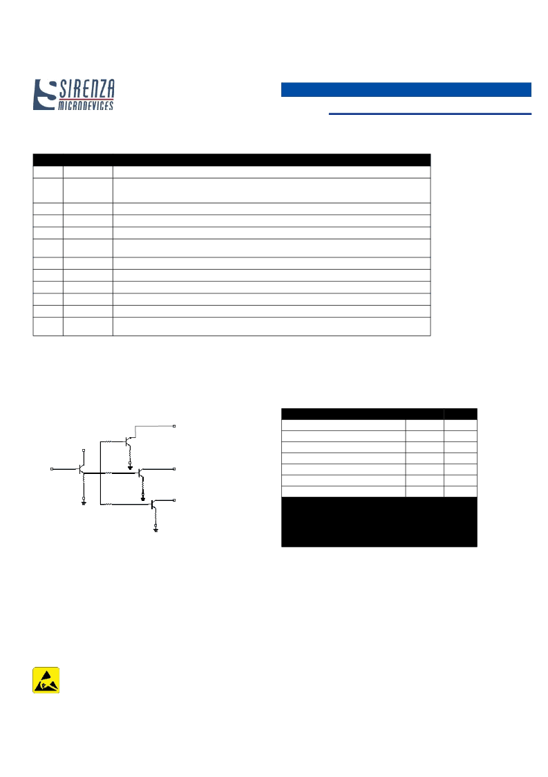
Simplified Device Schematic
Absolute Maximum Ratings
Parameters
Value
Unit
Current
200
mA
Device Voltage (V
D
)
Power Dissipation
6.0
V
1.2
W
Operating Lead Temperature (T
L
)
RF Input Power
-40 to +85
oC
15
dBm
Storage Temperature Range
-40 to +150
oC
Operating Junction Temperature (T
J
)
Operation of this device beyond any one of these limits may
cause permanent damage. For reliable continuous operation
the device voltage and current must not exceed the maximum
operating values specified in the table on page one.
+150
oC
Bias conditions should also satisfy the following expression:
I
D
V
D
< (T
J
- T
L
) / R
TH’
j-l
RFout
RFout
RFout
RFin
相关PDF资料 |
PDF描述 |
|---|---|
| CGA-0116Z | 3-Output Active Splitter for CATV |
| CGA-3318Z | Dual CATV Broadband High Linearity SiGe HBT Amplifier |
| CGA-6618Z | Dual CATV 1 MHz to 1000 MHz High Linearity GaAs HBT Amplifier |
| CGAT | Adhesive lined polyolefin heat-shrinkable tubing |
| CGB-1089Z | 50 - 1000 MHz Single Ended InGaP/GaAs HBT MMIC CATV Amplifier |
相关代理商/技术参数 |
参数描述 |
|---|---|
| CGA-0116Z | 制造商:RF Micro Devices Inc 功能描述:IC CATV SPLITTER 3-OUT 16-TSSOP |
| CGA016X368L | 制造商:n/a 功能描述:747D683M016AL2AS S9L2A |
| CGA020X323L | 制造商:n/a 功能描述:747D233M020AL2AS |
| CGA035X313M | 制造商:n/a 功能描述:747D113M035AMLAS S9I3A |
| CGA0402MLC-05G | 制造商:Bourns Inc 功能描述:ESD Suppressors Chip Guard 0402 5 Volt |
发布紧急采购,3分钟左右您将得到回复。