参数资料
| 型号: | CM1215-02SO |
| 厂商: | ON Semiconductor |
| 文件页数: | 5/9页 |
| 文件大小: | 0K |
| 描述: | 2 CH ESD SOT 23 |
| 产品变化通告: | Product Obsolescence 04/Nov/2010 |
| 标准包装: | 3,000 |
| 电极标记: | 2 通道阵列 - 双向 |
| 安装类型: | 表面贴装 |
| 封装/外壳: | TO-236-3,SC-59,SOT-23-3 |
| 供应商设备封装: | SOT-23-3 |
| 包装: | 带卷 (TR) |
�� �
�
�CM1215�
�APPLICATION� INFORMATION�
�Design� Considerations�
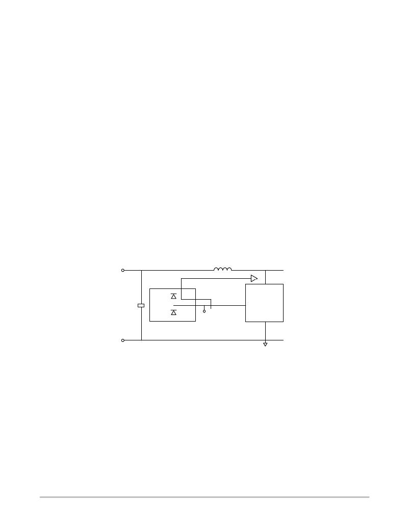
�In� order� to� realize� the� maximum� protection� against� ESD� pulses,� care� must� be� taken� in� the� PCB� layout� to� minimize� parasitic�
�series� inductances� on� the� Supply/� Ground� rails� as� well� as� the� signal� trace� segment� between� the� signal� input� (typically�
�a� connector)� and� the� ESD� protection� device.� Refer� to� Figure� 1,� which� illustrates� an� example� of� a� positive� ESD� pulse� striking�
�an� input� channel.� The� parasitic� series� inductance� back� to� the� power� supply� is� represented� by� L1� and� L2.� The� voltage� VCL� on�
�the� line� being� protected� is:�
�V� CL� =� Fwd� voltage� drop� of� D� 1� +� V� SUPPLY� +� L1� x� d(I� ESD� )� /� dt+� L2� x� d(IESD)� /� dt�
�where� IESD� is� the� ESD� current� pulse,� and� VSUPPLY� is� the� positive� supply� voltage.�
�An� ESD� current� pulse� can� rise� from� zero� to� its� peak� value� in� a� very� short� time.� As� an� example,� a� level� 4� contact� discharge�
�per� the� IEC61000� ?� 4� ?� 2� standard� results� in� a� current� pulse� that� rises� from� zero� to� 30� Amps� in� 1ns.� Here� d(IESD)/dt� can� be�
�approximated� by� d(� ESD� )/dt,� or� 30/(1x10� ?� 9).� So� just� 10� nH� of� series� inductance� (L1� and� L2� combined)� will� lead� to� a� 300� V�
�increment� in� VCL!�
�Similarly� for� negative� ESD� pulses,� parasitic� series� inductance� from� the� V� N� pin� to� the� ground� rail� will� lead� to� drastically�
�increased� negative� voltage� on� the� line� being� protected.�
�As� a� general� rule,� the� ESD� Protection� Array� should� be� located� as� close� as� possible� to� the� point� of� entry� of� expected�
�electrostatic� discharges.� The� power� supply� bypass� capacitor� mentioned� above� should� be� as� close� to� the� V� P� pin� of� the� Protection�
�Array� as� possible,� with� minimum� PCB� trace� lengths� to� the� power� supply,� ground� planes� and� between� the� signal� input� and� the�
�ESD� device� to� minimize� stray� series� inductance.�
�Additional� Information�
�See� also� ON� Semiconductor� Application� Note,� “Design� Considerations� for� ESD� Protection”,� in� the� Applications� section.�
�L1�
�POSITIVE� SUPPLY�
�PATH� OF� ESD� CURRENT�
�PULSE� (IESD)�
�C1�
�D1�
�ONE�
�CHANNEL�
�D2�
�LINE� BEING�
�PROTECTED�
�CHANNEL�
�IMPUT�
�SYSTEM� OR�
�CIRCUITRY�
�BEING�
�PROTECTED�
�GROUND� RAIL�
�CHASSI‘S� GROUND�
�Figure� 3.� Application� of� Positive� ESD� Pulse� between� Input� Channel� and� Ground�
�http://onsemi.com�
�5�
�相关PDF资料 |
PDF描述 |
|---|---|
| LTC6101CHS5#TRPBF | IC AMP CURRENT SENSE TSOT23-5 |
| CM1215-02SR | 2 CH ESD SOT-143 |
| NPPN062AFCN-RC | CONN RECEPT 2MM DUAL STR 12POS |
| AA1-F0-10-620-1B1-C | A SERIES 1 POLE CURR RELAY 5 AMP |
| MMK23-0441H1 | CONN RACK/PANEL 44POS 5A |
相关代理商/技术参数 |
参数描述 |
|---|---|
| CM1215-02SR | 功能描述:ESD 抑制器 2-ch. ESD Protection RoHS:否 制造商:STMicroelectronics 通道:8 Channels 击穿电压:8 V 电容:45 pF 端接类型:SMD/SMT 封装 / 箱体:uQFN-16 功率耗散 Pd: 工作温度范围:- 40 C to + 85 C |
| CM1215-02SS | 制造商:CALMIRCO 制造商全称:California Micro Devices Corp 功能描述:1-, 2- and 4-Channel Low Capacitance ESD Arrays |
| CM1215-02ST | 制造商:CALMIRCO 制造商全称:California Micro Devices Corp 功能描述:1-, 2- and 4-Channel Low Capacitance ESD Arrays |
| CM1215-04SO | 功能描述:ESD 抑制器 4-ch. ESD Protection RoHS:否 制造商:STMicroelectronics 通道:8 Channels 击穿电压:8 V 电容:45 pF 端接类型:SMD/SMT 封装 / 箱体:uQFN-16 功率耗散 Pd: 工作温度范围:- 40 C to + 85 C |
| CM1215-04ST | 制造商:CALMIRCO 制造商全称:California Micro Devices Corp 功能描述:1-, 2- and 4-Channel Low Capacitance ESD Arrays |
发布紧急采购,3分钟左右您将得到回复。