参数资料
| 型号: | CM1224-04SO |
| 厂商: | ON Semiconductor |
| 文件页数: | 6/11页 |
| 文件大小: | 0K |
| 描述: | TVS ARRAY ESD LOW 2CH SOT23-6 |
| 标准包装: | 3,000 |
| 电压 - 反向隔离(标准值): | 3.3V |
| 电压 - 击穿: | 6V |
| 电极标记: | 4 通道阵列 - 双向 |
| 安装类型: | 表面贴装 |
| 封装/外壳: | SOT-23-6 |
| 供应商设备封装: | SOT-23-6 |
| 包装: | 带卷 (TR) |
�� �
�
�CM1224�
�APPLICATION� INFORMATION�
�Design� Considerations�
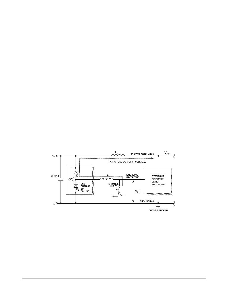
�To� realize� the� maximum� protection� against� ESD� pulses,� care� must� be� taken� in� the� PCB� layout� to� minimize� parasitic� series�
�inductances� on� the� Supply/� Ground� rails� as� well� as� the� signal� trace� segment� between� the� signal� input� (typically� a� connector)�
�and� the� ESD� protection� device.� Figure� 3� illustrates� an� example� of� a� positive� ESD� pulse� striking� an� input� channel.� The� parasitic�
�series� inductance� back� to� the� power� supply� is� represented� by� L� 1� and� L� 2� .� The� voltage� V� CL� on� the� line� being� protected� is:�
�V� CL� =� Fwd� voltage� drop� of� D� 1� +� V� SUPPLY� +� L� 1� x� d(I� ESD� )� /� dt� +� L� 2� x� d(I� ESD� )� /� dt�
�where� I� ESD� is� the� ESD� current� pulse,� and� V� SUPPLY� is� the� positive� supply� voltage.�
�An� ESD� current� pulse� can� rise� from� zero� to� its� peak� value� in� a� very� short� time.� As� an� example,� a� level� 4� contact� discharge�
�per� the� IEC61000� ?� 4� ?� 2� standard� results� in� a� current� pulse� that� rises� from� 0� to� 30� Amps� in� 1ns.� Here� d(I� ESD� )/dt� can� be�
�approximated� by� Δ� I� ESD� /� Δ� t,� or� 30/(1x10� ?� 9� ).� So� just� 10� nH� of� series� inductance� (L� 1� and� L� 2� combined)� will� lead� to� a� 300� V�
�increment� in� V� CL� !�
�Similarly� for� negative� ESD� pulses,� parasitic� series� inductance� from� the� V� N� pin� to� the� ground� rail� will� lead� to� drastically�
�increased� negative� voltage� on� the� line� being� protected.�
�The� CM1224� has� an� integrated� Zener� diode� between� V� P� and� V� N� .� This� greatly� reduces� the� effect� of� supply� rail� inductance�
�L� 2� on� V� CL� by� clamping� V� P� at� the� breakdown� voltage� of� the� Zener� diode.� However,� for� the� lowest� possible� V� CL� ,� especially� when�
�V� P� is� biased� at� a� voltage� significantly� below� the� Zener� breakdown� voltage,� it� is� recommended� that� a� 0.22� m� F� ceramic� chip�
�capacitor� be� connected� between� V� P� and� the� ground� plane.�
�As� a� general� rule,� the� ESD� Protection� Array� should� be� located� as� close� as� possible� to� the� point� of� entry� of� expected�
�electrostatic� discharges.� The� power� supply� bypass� capacitor� mentioned� earlier� should� be� as� close� to� the� V� P� pin� of� the� Protection�
�Array� as� possible,� with� minimum� PCB� trace� lengths� to� the� power� supply,� ground� planes� and� between� the� signal� input� and� the�
�ESD� device� to� minimize� stray� series� inductance.�
�Additional� Information�
�See� also� ON� Semiconductor� Application� Note� “Design� Considerations� for� ESD� Protection”.�
�Figure� 3.� Application� of� Positive� ESD� Pulse� between� Input� Channel� and� Ground�
�http://onsemi.com�
�6�
�相关PDF资料 |
PDF描述 |
|---|---|
| 168447032001025 | CONNECTOR HEADER 32POS R/A |
| RNCP1206FTD475R | RES 475 OHM 1/2W 1% 1206 SMD |
| 108557096008025 | CONNECTOR HEADER 96POS R/A |
| 208457048001049 | CONNECTOR RECEPT 48POS STR |
| RNCP1206FTD33R2 | RES 33.2 OHM 1/2W 1% 1206 SMD |
相关代理商/技术参数 |
参数描述 |
|---|---|
| CM1224K | 制造商:CML 制造商全称:Chicago Miniature Lamp,inc 功能描述:R-12 Single Contact Bayonet Base |
| CM1225 | 制造商:ONSEMI 制造商全称:ON Semiconductor 功能描述:4-Channel Low Capacitance ESD Protection Arrays |
| CM-1225 | 功能描述:机架和机柜配件 1.75"X19" CBL/PANEL RoHS:否 制造商:Bivar 产品:Rack Accessories 面板空间: 颜色:Black |
| CM1225-04DE | 功能描述:ESD 抑制器 4-ch ESD Protection 0.7pF Capacitance RoHS:否 制造商:STMicroelectronics 通道:8 Channels 击穿电压:8 V 电容:45 pF 端接类型:SMD/SMT 封装 / 箱体:uQFN-16 功率耗散 Pd: 工作温度范围:- 40 C to + 85 C |
| CM1226-04DE | 功能描述:ESD 抑制器 4-ch ESD Protection 0.7pF Capacitance RoHS:否 制造商:STMicroelectronics 通道:8 Channels 击穿电压:8 V 电容:45 pF 端接类型:SMD/SMT 封装 / 箱体:uQFN-16 功率耗散 Pd: 工作温度范围:- 40 C to + 85 C |
发布紧急采购,3分钟左右您将得到回复。