参数资料
| 型号: | CM1293A-02SO |
| 厂商: | ON Semiconductor |
| 文件页数: | 6/9页 |
| 文件大小: | 0K |
| 描述: | ESD PROT LOW CAP 2CH SC-74 |
| 标准包装: | 3,000 |
| 电压 - 反向隔离(标准值): | 3.3V |
| 电压 - 击穿: | 6V |
| 电极标记: | 2 通道阵列 - 双向 |
| 安装类型: | 表面贴装 |
| 封装/外壳: | SC-74,SOT-457 |
| 供应商设备封装: | SC-74 |
| 包装: | 带卷 (TR) |
�� �
�
�CM1293A�
�APPLICATION� INFORMATION�
�Design� Considerations�
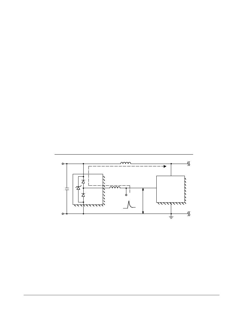
�In� order� to� realize� the� maximum� protection� against� ESD� pulses,� care� must� be� taken� in� the� PCB� layout� to� minimize� parasitic�
�series� inductances� on� the� Supply/Ground� rails� as� well� as� the� signal� trace� segment� between� the� signal� input� (typically� a�
�connector)� and� the� ESD� protection� device.� Refer� to� Figure� 5,� which� illustrates� an� example� of� a� positive� ESD� pulse� striking� an�
�input� channel.� The� parasitic� series� inductance� back� to� the� power� supply� is� represented� by� L� 1� and� L� 2� .� The� voltage� V� CL� on� the�
�line� being� protected� is:�
�V� CL� =� Fwd� voltage� drop� of� D� 1� +� V� SUPPLY� +� L� 1� x� d(I� ESD� )� /� dt+� L� 2� x� d(I� ESD� )� /� dt�
�where� I� ESD� is� the� ESD� current� pulse,� and� V� SUPPLY� is� the� positive� supply� voltage.�
�An� ESD� current� pulse� can� rise� from� zero� to� its� peak� value� in� a� very� short� time.� As� an� example,� a� level� 4� contact� discharge�
�per� the� IEC61000� ?� 4� ?� 2� standard� results� in� a� current� pulse� that� rises� from� zero� to� 30� Amps� in� 1� ns.� Here� d(I� ESD� )/dt� can� be�
�approximated� by� D� I� ESD� /� D� t,� or� 30/(1x10� ?� 9� ).� So� just� 10� nH� of� series� inductance� (L� 1� and� L� 2� combined)� will� lead� to� a� 300� V�
�increment� in� V� CL� !�
�Similarly� for� negative� ESD� pulses,� parasitic� series� inductance� from� the� V� N� pin� to� the� ground� rail� will� lead� to� drastically�
�increased� negative� voltage� on� the� line� being� protected.�
�The� CM1293� has� an� integrated� Zener� diode� between� V� P� and� V� N� .� This� greatly� reduces� the� effect� of� supply� rail� inductance�
�L� 2� on� V� CL� by� clamping� V� P� at� the� breakdown� voltage� of� the� Zener� diode.� However,� for� the� lowest� possible� V� CL� ,� especially� when�
�V� P� is� biased� at� a� voltage� significantly� below� the� Zener� breakdown� voltage,� it� is� recommended� that� a� 0.22� μ� F� ceramic� chip�
�capacitor� be� connected� between� V� P� and� the� ground� plane.�
�As� a� general� rule,� the� ESD� Protection� Array� should� be� located� as� close� as� possible� to� the� point� of� entry� of� expected�
�electrostatic� discharges.� The� power� supply� bypass� capacitor� mentioned� above� should� be� as� close� to� the� V� P� pin� of� the� Protection�
�Array� as� possible,� with� minimum� PCB� trace� lengths� to� the� power� supply,� ground� planes� and� between� the� signal� input� and� the�
�ESD� device� to� minimize� stray� series� inductance.�
�V� P�
�L� 2�
�POSITIVE� SUPPLY� RAIL�
�V� CC�
�PATH� OF� ESD� CURRENT� PULSE� I� ESO�
�0.22� m� F�
�D� 1�
�D� 2�
�ONE�
�CHANNEL�
�L� 1�
�CHANNEL�
�INPUT�
�25� A�
�LINE� BEING�
�PROTECTED�
�V� CL�
�SYSTEM� OR�
�CIRCUITRY�
�BEING�
�PROTECTED�
�0A�
�V� N�
�GROUND� RAIL�
�CHASSIS� GROUND�
�Figure� 5.� Application� of� Positive� ESD� Pulse� between� Input� Channel� and� Ground�
�http://onsemi.com�
�6�
�相关PDF资料 |
PDF描述 |
|---|---|
| CRCW04021R60FKED | RES 1.60 OHM 1/16W 1% 0402 SMD |
| 170183-1 | CONN UNINS RECPT 18-22AWG 0.250 |
| SMF24CT1G | IC TVS ARRAY 5LINE 100W SOT-363 |
| 961222-5500-AR-TP | CONN HEADER R/A 22POS GOLD SMD |
| 03540604ZXGY | FUSE BLOCK 3AG 4POS 3/16"QC NEMA |
相关代理商/技术参数 |
参数描述 |
|---|---|
| CM1293A-02SR | 功能描述:ESD 抑制器 2-ch. 8KV/1pF Ultra RoHS:否 制造商:STMicroelectronics 通道:8 Channels 击穿电压:8 V 电容:45 pF 端接类型:SMD/SMT 封装 / 箱体:uQFN-16 功率耗散 Pd: 工作温度范围:- 40 C to + 85 C |
| CM1293A-04MR | 功能描述:ESD 抑制器 4-ch.Low Capacitance RoHS:否 制造商:STMicroelectronics 通道:8 Channels 击穿电压:8 V 电容:45 pF 端接类型:SMD/SMT 封装 / 箱体:uQFN-16 功率耗散 Pd: 工作温度范围:- 40 C to + 85 C |
| CM1293A-04SO | 功能描述:ESD 抑制器 4-ch.Low Capacitance RoHS:否 制造商:STMicroelectronics 通道:8 Channels 击穿电压:8 V 电容:45 pF 端接类型:SMD/SMT 封装 / 箱体:uQFN-16 功率耗散 Pd: 工作温度范围:- 40 C to + 85 C |
| CM1295 | 制造商:CML 制造商全称:Chicago Miniature Lamp,inc 功能描述:S-8 Single Contact Bayonet Base |
| CM12A | 制造商:CML 制造商全称:Chicago Miniature Lamp,inc 功能描述:T-2 Telephone Slide Base - Type 5 (short) |
发布紧急采购,3分钟左右您将得到回复。