参数资料
| 型号: | COP8CDR9LVA8 |
| 厂商: | National Semiconductor |
| 文件页数: | 48/111页 |
| 文件大小: | 0K |
| 描述: | IC MCU CMOS 8BIT 68-PLCC |
| 标准包装: | 18 |
| 系列: | COP8™ 8C |
| 核心处理器: | COP8 |
| 芯体尺寸: | 8-位 |
| 速度: | 20MHz |
| 连通性: | Microwire/Plus(SPI),UART/USART |
| 外围设备: | POR,PWM,WDT |
| 输入/输出数: | 59 |
| 程序存储器容量: | 32KB(32K x 8) |
| 程序存储器类型: | 闪存 |
| RAM 容量: | 1K x 8 |
| 电压 - 电源 (Vcc/Vdd): | 2.7 V ~ 5.5 V |
| 数据转换器: | A/D 16x10b |
| 振荡器型: | 内部 |
| 工作温度: | -40°C ~ 85°C |
| 封装/外壳: | 68-LCC(J 形引线) |
| 包装: | 管件 |
| 其它名称: | *COP8CDR9LVA8 |
第1页第2页第3页第4页第5页第6页第7页第8页第9页第10页第11页第12页第13页第14页第15页第16页第17页第18页第19页第20页第21页第22页第23页第24页第25页第26页第27页第28页第29页第30页第31页第32页第33页第34页第35页第36页第37页第38页第39页第40页第41页第42页第43页第44页第45页第46页第47页当前第48页第49页第50页第51页第52页第53页第54页第55页第56页第57页第58页第59页第60页第61页第62页第63页第64页第65页第66页第67页第68页第69页第70页第71页第72页第73页第74页第75页第76页第77页第78页第79页第80页第81页第82页第83页第84页第85页第86页第87页第88页第89页第90页第91页第92页第93页第94页第95页第96页第97页第98页第99页第100页第101页第102页第103页第104页第105页第106页第107页第108页第109页第110页第111页
SNOS535I – OCTOBER 2000 – REVISED MARCH 2013
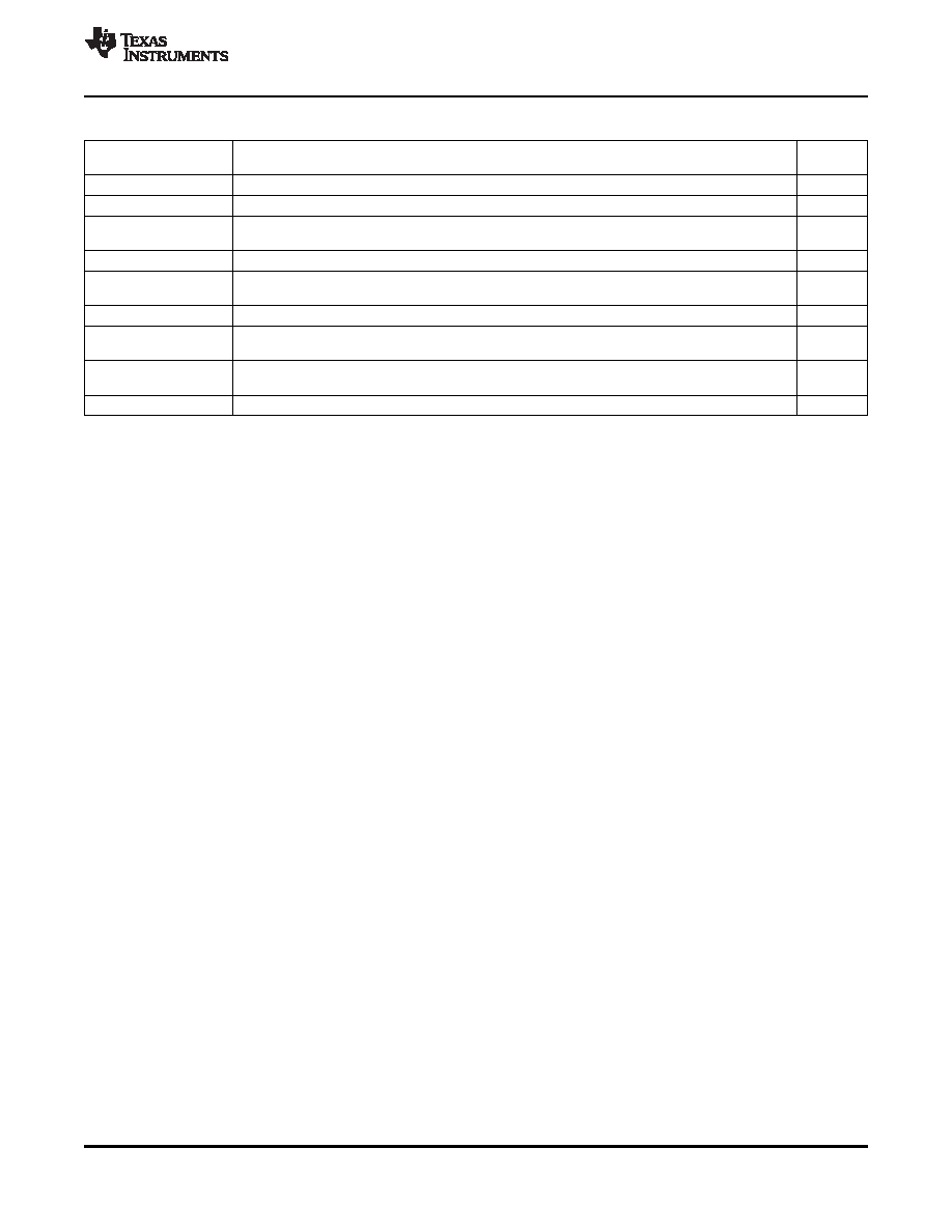
Table 5-11. Register and Bit Name Definitions
Register
RAM
Purpose
Name
Location
ISPADHI
High byte of Flash Memory Address
0xA9
ISPADLO
Low byte of Flash Memory Address
0xA8
ISPWR
The user must store the byte to be written into this register before jumping into the write byte
0xAB
routine.
ISPRD
Data will be returned to this register after the read byte routine execution.
0xAA
ISPKEY
The ISPKEY Register is required to validate the JSRB instruction and must be loaded within 6
0xE2
instruction cycles before the JSRB.
BYTECOUNTLO
Holds the count of the number of bytes to be read or written in block operations.
0xF1
PGMTIM
Write Timing Register. This register must be loaded, by the user, with the proper value before
0xE1
execution of any USER ISP Write or Erase operation. Refer to Table 5-7 for the correct value.
Confirmation Code
The user must place this code in the accumulator before execution of a Flash Memory Mass Erase
A
command.
KEY
Must be transferred to the ISPKEY register before execution of a JSRB instruction.
0x98
5.10.9 RESTRICTIONS ON SOFTWARE WHEN CALLING ISP ROUTINES IN BOOT ROM
1. The hardware will disable interrupts from occurring. The hardware will leave the GIE bit in its current
state, and if set, the hardware interrupts will occur when execution is returned to Flash Memory.
Subsequent interrupts, during ISP operation, from the same interrupt source will be lost. Interrupts
may occur between setting the KEY and executing the JSRB instruction. In this case, the KEY
will expire before the JSRB is executed. It is, therefore, recommended that the software globally
disable interrupts before setting the Key.
2. The security feature in the MICROWIRE/PLUS ISP is ensured by software and not hardware. When
executing the MICROWIRE/PLUS ISP routine, the security bit is checked prior to performing all
instructions. Only the mass erase command, write PGMTIM register, and reading the Option register is
permitted within the MICROWIRE/PLUS ISP routine. When the user is performing his own ISP, all
commands are permitted. The entry points from the user's ISP code do not check for security. It is the
burden of the user to ensure his own security. See the Security bit description in Option Register for
more details on security.
3. When using any of the ISP functions in Boot ROM, the ISP routines will service the WATCHDOG
within the selected upper window. Upon return to flash memory, the WATCHDOG is serviced, the
lower window is enabled, and the user can service the WATCHDOG anytime following exit from Boot
ROM, but must service it within the selected upper window to avoid a WATCHDOG error.
4. Block Writes can start anywhere in the page of Flash memory, but cannot cross half page or full page
boundaries.
5. The user must ensure that a page erase or a mass erase is executed between two consecutive
writes to the same location in Flash memory. Two writes to the same location without an
intervening erase will produce unpredicatable results including possible disturbance of
unassociated locations.
5.10.10 FLASH MEMORY DURABILITY CONSIDERATIONS
The endurance of the Flash Memory (number of possible Erase/Write cycles) is a function of the erase
time and the lowest temperature at which the erasure occurs. If the device is to be used at low
temperature, additional erase operations can be used to extend the erase time. The user can determine
how many times to erase a page based on what endurance is desired for the application (e.g. four page
erase cycles, each time a page erase is done, may be required to achieve the typical 100k Erase/Write
cycles in an application which may be operating down to 0°C). Also, the customer can verify that the entire
page is erased, with software, and request additional erase operations if desired.
Copyright 2000–2013, Texas Instruments Incorporated
Functional Description
41
相关PDF资料 |
PDF描述 |
|---|---|
| MC68HC705JJ7CDW | IC MCU 8BIT 20-SOIC |
| C8051F583-IQ | IC 8051 MCU 128K FLASH 32-QFP |
| 67068-0000 | CONN USB RT ANG RECPT TYPE B BLK |
| P89LPC952FBD,157 | IC 80C51 MCU FLASH 8K 44-LQFD |
| LPC11C22FBD48/301, | IC MCU 32BIT 16KB FLASH 48LQFP |
相关代理商/技术参数 |
参数描述 |
|---|---|
| COP8CFE9 | 制造商:NSC 制造商全称:National Semiconductor 功能描述:8-Bit CMOS Flash Microcontroller with 8k Memory, Virtual EEPROM, and 10-Bit A/D |
| COP8CFE9HLQ9 | 功能描述:IC MCU FLASH 8BIT 8K A/D 44LLP RoHS:是 类别:集成电路 (IC) >> 嵌入式 - 微控制器, 系列:COP8™ 8C 标准包装:250 系列:56F8xxx 核心处理器:56800E 芯体尺寸:16-位 速度:60MHz 连通性:CAN,SCI,SPI 外围设备:POR,PWM,温度传感器,WDT 输入/输出数:21 程序存储器容量:40KB(20K x 16) 程序存储器类型:闪存 EEPROM 大小:- RAM 容量:6K x 16 电压 - 电源 (Vcc/Vdd):2.25 V ~ 3.6 V 数据转换器:A/D 6x12b 振荡器型:内部 工作温度:-40°C ~ 125°C 封装/外壳:48-LQFP 包装:托盘 配用:MC56F8323EVME-ND - BOARD EVALUATION MC56F8323 |
| COP8CFE9HVA9/NOPB | 功能描述:IC MCU EEPROM 8BIT 8K 44-PLCC RoHS:是 类别:集成电路 (IC) >> 嵌入式 - 微控制器, 系列:COP8™ 8C 标准包装:250 系列:56F8xxx 核心处理器:56800E 芯体尺寸:16-位 速度:60MHz 连通性:CAN,SCI,SPI 外围设备:POR,PWM,温度传感器,WDT 输入/输出数:21 程序存储器容量:40KB(20K x 16) 程序存储器类型:闪存 EEPROM 大小:- RAM 容量:6K x 16 电压 - 电源 (Vcc/Vdd):2.25 V ~ 3.6 V 数据转换器:A/D 6x12b 振荡器型:内部 工作温度:-40°C ~ 125°C 封装/外壳:48-LQFP 包装:托盘 配用:MC56F8323EVME-ND - BOARD EVALUATION MC56F8323 |
| COP8CFE9IMT9/NOPB | 功能描述:IC MCU EEPROM 8BIT 8K 48-TSSOP RoHS:是 类别:集成电路 (IC) >> 嵌入式 - 微控制器, 系列:COP8™ 8C 标准包装:250 系列:56F8xxx 核心处理器:56800E 芯体尺寸:16-位 速度:60MHz 连通性:CAN,SCI,SPI 外围设备:POR,PWM,温度传感器,WDT 输入/输出数:21 程序存储器容量:40KB(20K x 16) 程序存储器类型:闪存 EEPROM 大小:- RAM 容量:6K x 16 电压 - 电源 (Vcc/Vdd):2.25 V ~ 3.6 V 数据转换器:A/D 6x12b 振荡器型:内部 工作温度:-40°C ~ 125°C 封装/外壳:48-LQFP 包装:托盘 配用:MC56F8323EVME-ND - BOARD EVALUATION MC56F8323 |
| COP8CJ20 WAF | 制造商:Texas Instruments 功能描述: |
发布紧急采购,3分钟左右您将得到回复。