- 您现在的位置:买卖IC网 > PDF目录379960 > COP8SGE740N7 (NATIONAL SEMICONDUCTOR CORP) LP2950/LP2951 Series of Adjustable Micropower Voltage Regulators; Package: TO-252; No of Pins: 3 PDF资料下载
参数资料
| 型号: | COP8SGE740N7 |
| 厂商: | NATIONAL SEMICONDUCTOR CORP |
| 元件分类: | 微控制器/微处理器 |
| 英文描述: | LP2950/LP2951 Series of Adjustable Micropower Voltage Regulators; Package: TO-252; No of Pins: 3 |
| 中文描述: | 8-BIT, OTPROM, 10 MHz, MICROCONTROLLER, PDIP40 |
| 封装: | DIP-40 |
| 文件页数: | 23/62页 |
| 文件大小: | 913K |
| 代理商: | COP8SGE740N7 |
第1页第2页第3页第4页第5页第6页第7页第8页第9页第10页第11页第12页第13页第14页第15页第16页第17页第18页第19页第20页第21页第22页当前第23页第24页第25页第26页第27页第28页第29页第30页第31页第32页第33页第34页第35页第36页第37页第38页第39页第40页第41页第42页第43页第44页第45页第46页第47页第48页第49页第50页第51页第52页第53页第54页第55页第56页第57页第58页第59页第60页第61页第62页
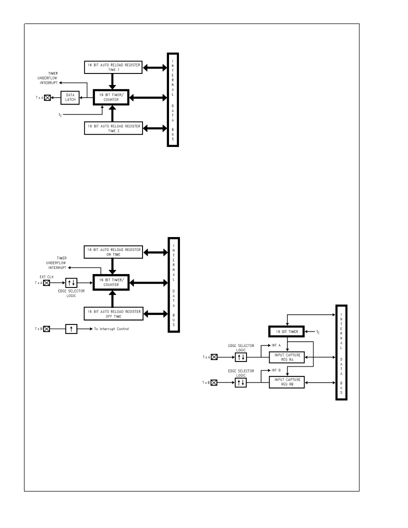
6.0 Timers
(Continued)
In this mode the input pin TxB can be used as an indepen-
dent positive edge sensitive interrupt input if the TxENB
control flag is set. The occurrence of a positive edge on the
TxB input pin is latched into the TxPNDB flag.
Figure 16 shows a block diagram of the timer in External
Event Counter mode.
Note:
The PWM output is not available in this mode since the TxApin is being
used as the counter input clock.
6.2.3 Mode 3. Input Capture Mode
Each device can precisely measure external frequencies or
time external events by placing the timer block, Tx, in the
input capture mode. In this mode, the reload registers serve
as independent capture registers, capturing the contents of
the timer when an external event occurs (transition on the
timer input pin). The capture registers can be read while
maintaining count, a feature that lets the user measure
elapsed time and time between events. By saving the timer
value when the external event occurs, the time of the exter-
nal event is recorded. Most microcontrollers have a latency
time because they cannot determine the timer value when
the external event occurs. The capture register eliminates
the latency time, thereby allowing the applications program
to retrieve the timer value stored in the capture register.
In this mode, the timer Tx is constantly running at the fixed t
C
rate. The two registers, RxA and RxB, act as capture regis-
ters. Each register acts in conjunction with a pin. The register
RxAacts in conjunction with the TxApin and the register RxB
acts in conjunction with the TxB pin.
The timer value gets copied over into the register when a
trigger event occurs on its corresponding pin. Control bits,
TxC3, TxC2 and TxC1, allow the trigger events to be speci-
fied either as a positive or a negative edge. The trigger
condition for each input pin can be specified independently.
The trigger conditions can also be programmed to generate
interrupts. The occurrence of the specified trigger condition
on the TxA and TxB pins will be respectively latched into the
pending flags, TxPNDA and TxPNDB. The control flag Tx-
ENA allows the interrupt on TxA to be either enabled or
disabled. Setting the TxENA flag enables interrupts to be
generated when the selected trigger condition occurs on the
TxA pin. Similarly, the flag TxENB controls the interrupts
from the TxB pin.
Underflows from the timer can also be programmed to gen-
erate interrupts. Underflows are latched into the timer TxC0
pending flag (the TxC0 control bit serves as the timer under-
flow interrupt pending flag in the Input Capture mode). Con-
sequently, the TxC0 control bit should be reset when enter-
ing the Input Capture mode. The timer underflow interrupt is
enabled with the TxENA control flag. When a TxA interrupt
occurs in the Input Capture mode, the user must check both
the TxPNDA and TxC0 pending flags in order to determine
whether a TxA input capture or a timer underflow (or both)
caused the interrupt.
Figure 17 shows a block diagram of the timer T1 in Input
Capture mode. Timer T2 and T3 are identical to T1.
10131746
FIGURE 15. Timer in PWM Mode
10131747
FIGURE 16. Timer in External Event Counter Mode
10131748
FIGURE 17. Timer in Input Capture Mode
C
www.national.com
23
相关PDF资料 |
PDF描述 |
|---|---|
| COP8SGE740N8 | LP2950/LP2951 Series of Adjustable Micropower Voltage Regulators; Package: TO-252; No of Pins: 3 |
| COP8SGE740N9 | LP2950/LP2951 Series of Adjustable Micropower Voltage Regulators; Package: TO-92; No of Pins: 3 |
| COP8SGE740Q3 | LP2950/LP2951 Series of Adjustable Micropower Voltage Regulators; Package: TO-92; No of Pins: 3 |
| COP8SGE740Q6 | LP2950/LP2951 Series of Adjustable Micropower Voltage Regulators; Package: TO-92; No of Pins: 3 |
| COP8SGE740Q7 | LP2950/LP2951 Series of Adjustable Micropower Voltage Regulators; Package: SOIC NARROW; No of Pins: 8 |
相关代理商/技术参数 |
参数描述 |
|---|---|
| COP8SGE740N8 | 功能描述:IC MCU 8BIT CMOS OTP 40DIP RoHS:否 类别:集成电路 (IC) >> 嵌入式 - 微控制器, 系列:COP8™ 8SG 其它有关文件:STM32F101T8 View All Specifications 特色产品:STM32 32-bit Cortex MCUs 标准包装:490 系列:STM32 F1 核心处理器:ARM? Cortex?-M3 芯体尺寸:32-位 速度:36MHz 连通性:I²C,IrDA,LIN,SPI,UART/USART 外围设备:DMA,PDR,POR,PVD,PWM,温度传感器,WDT 输入/输出数:26 程序存储器容量:64KB(64K x 8) 程序存储器类型:闪存 EEPROM 大小:- RAM 容量:10K x 8 电压 - 电源 (Vcc/Vdd):2 V ~ 3.6 V 数据转换器:A/D 10x12b 振荡器型:内部 工作温度:-40°C ~ 85°C 封装/外壳:36-VFQFN,36-VFQFPN 包装:托盘 配用:497-10030-ND - STARTER KIT FOR STM32497-8853-ND - BOARD DEMO STM32 UNIV USB-UUSCIKSDKSTM32-PL-ND - KIT IAR KICKSTART STM32 CORTEXM3497-8512-ND - KIT STARTER FOR STM32F10XE MCU497-8505-ND - KIT STARTER FOR STM32F10XE MCU497-8304-ND - KIT STM32 MOTOR DRIVER BLDC497-6438-ND - BOARD EVALUTION FOR STM32 512K497-6289-ND - KIT PERFORMANCE STICK FOR STM32MCBSTM32UME-ND - BOARD EVAL MCBSTM32 + ULINK-MEMCBSTM32U-ND - BOARD EVAL MCBSTM32 + ULINK2更多... 其它名称:497-9032STM32F101T8U6-ND |
| COP8SGE740N8XXX/NOPB | 制造商:Texas Instruments 功能描述: |
| COP8SGE744V8 | 功能描述:8位微控制器 -MCU RoHS:否 制造商:Silicon Labs 核心:8051 处理器系列:C8051F39x 数据总线宽度:8 bit 最大时钟频率:50 MHz 程序存储器大小:16 KB 数据 RAM 大小:1 KB 片上 ADC:Yes 工作电源电压:1.8 V to 3.6 V 工作温度范围:- 40 C to + 105 C 封装 / 箱体:QFN-20 安装风格:SMD/SMT |
| COP8SGE744V8/NOPB | 功能描述:8位微控制器 -MCU RoHS:否 制造商:Silicon Labs 核心:8051 处理器系列:C8051F39x 数据总线宽度:8 bit 最大时钟频率:50 MHz 程序存储器大小:16 KB 数据 RAM 大小:1 KB 片上 ADC:Yes 工作电源电压:1.8 V to 3.6 V 工作温度范围:- 40 C to + 105 C 封装 / 箱体:QFN-20 安装风格:SMD/SMT |
| COP8SGE7HLQ8 | 功能描述:IC MCU OTP 8BIT 8K 2-COMP 44LLP RoHS:否 类别:集成电路 (IC) >> 嵌入式 - 微控制器, 系列:COP8™ 8SG 标准包装:250 系列:56F8xxx 核心处理器:56800E 芯体尺寸:16-位 速度:60MHz 连通性:CAN,SCI,SPI 外围设备:POR,PWM,温度传感器,WDT 输入/输出数:21 程序存储器容量:40KB(20K x 16) 程序存储器类型:闪存 EEPROM 大小:- RAM 容量:6K x 16 电压 - 电源 (Vcc/Vdd):2.25 V ~ 3.6 V 数据转换器:A/D 6x12b 振荡器型:内部 工作温度:-40°C ~ 125°C 封装/外壳:48-LQFP 包装:托盘 配用:MC56F8323EVME-ND - BOARD EVALUATION MC56F8323 |
发布紧急采购,3分钟左右您将得到回复。