- 您现在的位置:买卖IC网 > PDF目录169782 > COP8SGE744V8XXX (NATIONAL SEMICONDUCTOR CORP) 8-BIT, OTPROM, 15 MHz, MICROCONTROLLER, PQCC44 PDF资料下载
参数资料
| 型号: | COP8SGE744V8XXX |
| 厂商: | NATIONAL SEMICONDUCTOR CORP |
| 元件分类: | 微控制器/微处理器 |
| 英文描述: | 8-BIT, OTPROM, 15 MHz, MICROCONTROLLER, PQCC44 |
| 封装: | PLASTIC, LCC-44 |
| 文件页数: | 15/62页 |
| 文件大小: | 840K |
| 代理商: | COP8SGE744V8XXX |
第1页第2页第3页第4页第5页第6页第7页第8页第9页第10页第11页第12页第13页第14页当前第15页第16页第17页第18页第19页第20页第21页第22页第23页第24页第25页第26页第27页第28页第29页第30页第31页第32页第33页第34页第35页第36页第37页第38页第39页第40页第41页第42页第43页第44页第45页第46页第47页第48页第49页第50页第51页第52页第53页第54页第55页第56页第57页第58页第59页第60页第61页第62页
6.0 Timers (Continued)
Timing the width of the internal power-on-reset
The IDLE Timer T0 can generate an interrupt when the
twelfth bit toggles. This toggle is latched into the T0PND
pending flag, and will occur every 2.731 ms at the maximum
clock frequency (t
C = 0.67 s). A control flag T0EN allows the
interrupt from the twelfth bit of Timer T0 to be enabled or
disabled. Setting T0EN will enable the interrupt, while reset-
ting it will disable the interrupt.
6.2 TIMER T1, TIMER T2 and TIMER T3
Each device have a set of three powerful timer/counter
blocks, T1, T2 and T3. Since T1, T2, and T3 are identical, all
comments are equally applicable to any of the three timer
blocks which will be referred to as Tx.
Each timer block consists of a 16-bit timer, Tx, and two
supporting 16-bit autoreload/capture registers, RxA and
RxB. Each timer block has two pins associated with it, TxA
and TxB. The pin TxA supports I/O required by the timer
block, while the pin TxB is an input to the timer block. The
timer block has three operating modes: Processor Indepen-
dent PWM mode, External Event Counter mode, and Input
Capture mode.
The control bits TxC3, TxC2, and TxC1 allow selection of the
different modes of operation.
6.2.1 Mode 1. Processor Independent PWM Mode
One of the timer’s operating modes is the Processor Inde-
pendent PWM mode. In this mode, the timer generates a
“Processor Independent” PWM signal because once the
timer is setup, no more action is required from the CPU
which translates to less software overhead and greater
throughput. The user software services the timer block only
when the PWM parameters require updating. This capability
is provided by the fact that the timer has two separate 16-bit
reload registers. One of the reload registers contains the
“ON” timer while the other holds the “OFF” time. By contrast,
a microcontroller that has only a single reload register re-
quires an additional software to update the reload value
(alternate between the on-time/off-time).
The timer can generate the PWM output with the width and
duty cycle controlled by the values stored in the reload
registers. The reload registers control the countdown values
and the reload values are automatically written into the timer
when it counts down through 0, generating interrupt on each
reload. Under software control and with minimal overhead,
the PMW outputs are useful in controlling motors, triacs, the
intensity of displays, and in providing inputs for data acqui-
sition and sine wave generators.
In this mode, the timer Tx counts down at a fixed rate of t
C.
Upon every underflow the timer is alternately reloaded with
the contents of supporting registers, RxA and RxB. The very
first underflow of the timer causes the timer to reload from
the register RxA. Subsequent underflows cause the timer to
be reloaded from the registers alternately beginning with the
register RxB.
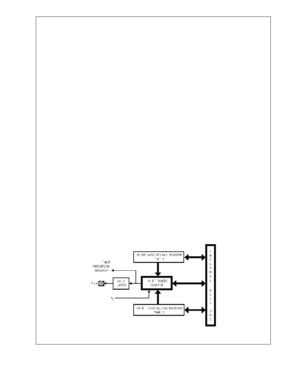
Figure 16 shows a block diagram of the timer in PWM mode.
The underflows can be programmed to toggle the TxA output
pin. The underflows can also be programmed to generate
interrupts.
Underflows from the timer are alternately latched into two
pending flags, TxPNDA and TxPNDB. The user must reset
these pending flags under software control. Two control
enable flags, TxENA and TxENB, allow the interrupts from
the timer underflow to be enabled or disabled. Setting the
timer enable flag TxENA will cause an interrupt when a timer
underflow causes the RxA register to be reloaded into the
timer. Setting the timer enable flag TxENB will cause an
interrupt when a timer underflow causes the RxB register to
be reloaded into the timer. Resetting the timer enable flags
will disable the associated interrupts.
Either or both of the timer underflow interrupts may be
enabled. This gives the user the flexibility of interrupting
once per PWM period on either the rising or falling edge of
the PWM output. Alternatively, the user may choose to inter-
rupt on both edges of the PWM output.
6.2.2 Mode 2. External Event Counter Mode
This mode is quite similar to the processor independent
PWM mode described above. The main difference is that the
timer, Tx, is clocked by the input signal from the TxA pin. The
Tx timer control bits, TxC3, TxC2 and TxC1 allow the timer to
be clocked either on a positive or negative edge from the
TxA pin. Underflows from the timer are latched into the
TxPNDA pending flag. Setting the TxENA control flag will
cause an interrupt when the timer underflows.
DS101317-46
FIGURE 16. Timer in PWM Mode
COP8SG
Family
www.national.com
22
相关PDF资料 |
PDF描述 |
|---|---|
| COP8SGE744V7XXX | 8-BIT, OTPROM, 10 MHz, MICROCONTROLLER, PQCC44 |
| COP8SGR740N7XXX | 8-BIT, OTPROM, 10 MHz, MICROCONTROLLER, PDIP40 |
| CP-1094-AST | PANEL MOUNT, CABLE TERMINATED, FEMALE, BNC CONNECTOR, SOLDER, RECEPTACLE |
| CP-1094-U | PANEL MOUNT, CABLE TERMINATED, FEMALE, BNC CONNECTOR, SOLDER, RECEPTACLE |
| CP-AD519 | PANEL MOUNT, CABLE TERMINATED, FEMALE, BNC CONNECTOR, SOLDER, RECEPTACLE |
相关代理商/技术参数 |
参数描述 |
|---|---|
| COP8SGE7HLQ8 | 功能描述:IC MCU OTP 8BIT 8K 2-COMP 44LLP RoHS:否 类别:集成电路 (IC) >> 嵌入式 - 微控制器, 系列:COP8™ 8SG 标准包装:250 系列:56F8xxx 核心处理器:56800E 芯体尺寸:16-位 速度:60MHz 连通性:CAN,SCI,SPI 外围设备:POR,PWM,温度传感器,WDT 输入/输出数:21 程序存储器容量:40KB(20K x 16) 程序存储器类型:闪存 EEPROM 大小:- RAM 容量:6K x 16 电压 - 电源 (Vcc/Vdd):2.25 V ~ 3.6 V 数据转换器:A/D 6x12b 振荡器型:内部 工作温度:-40°C ~ 125°C 封装/外壳:48-LQFP 包装:托盘 配用:MC56F8323EVME-ND - BOARD EVALUATION MC56F8323 |
| COP8SGE7VEJ7 | 制造商:Texas Instruments 功能描述: |
| COP8SGE7VEJ8 | 制造商:Rochester Electronics LLC 功能描述: 制造商:Texas Instruments 功能描述: |
| COP8SGE7VEJ8/NOPB | 功能描述:8位微控制器 -MCU RoHS:否 制造商:Silicon Labs 核心:8051 处理器系列:C8051F39x 数据总线宽度:8 bit 最大时钟频率:50 MHz 程序存储器大小:16 KB 数据 RAM 大小:1 KB 片上 ADC:Yes 工作电源电压:1.8 V to 3.6 V 工作温度范围:- 40 C to + 105 C 封装 / 箱体:QFN-20 安装风格:SMD/SMT |
| COP8SG-EPU | 功能描述:开发板和工具包 - 其他处理器 COP8SG EVAL/PROGAM UNIT RoHS:否 制造商:Freescale Semiconductor 产品:Development Systems 工具用于评估:P3041 核心:e500mc 接口类型:I2C, SPI, USB 工作电源电压: |
发布紧急采购,3分钟左右您将得到回复。