参数资料
| 型号: | CP82C55A |
| 厂商: | Intersil |
| 文件页数: | 20/29页 |
| 文件大小: | 0K |
| 描述: | IC I/O EXPANDER 24B 40DIP |
| 标准包装: | 9 |
| 接口: | 可编程 |
| 输入/输出数: | 24 |
| 中断输出: | 无 |
| 电源电压: | 4.5 V ~ 5.5 V |
| 工作温度: | 0°C ~ 70°C |
| 安装类型: | 通孔 |
| 封装/外壳: | 40-DIP(0.600",15.24mm) |
| 供应商设备封装: | 40-DIP |
| 包装: | 管件 |
| 产品目录页面: | 1236 (CN2011-ZH PDF) |
第1页第2页第3页第4页第5页第6页第7页第8页第9页第10页第11页第12页第13页第14页第15页第16页第17页第18页第19页当前第20页第21页第22页第23页第24页第25页第26页第27页第28页第29页
27
FN2969.10
November 16, 2006
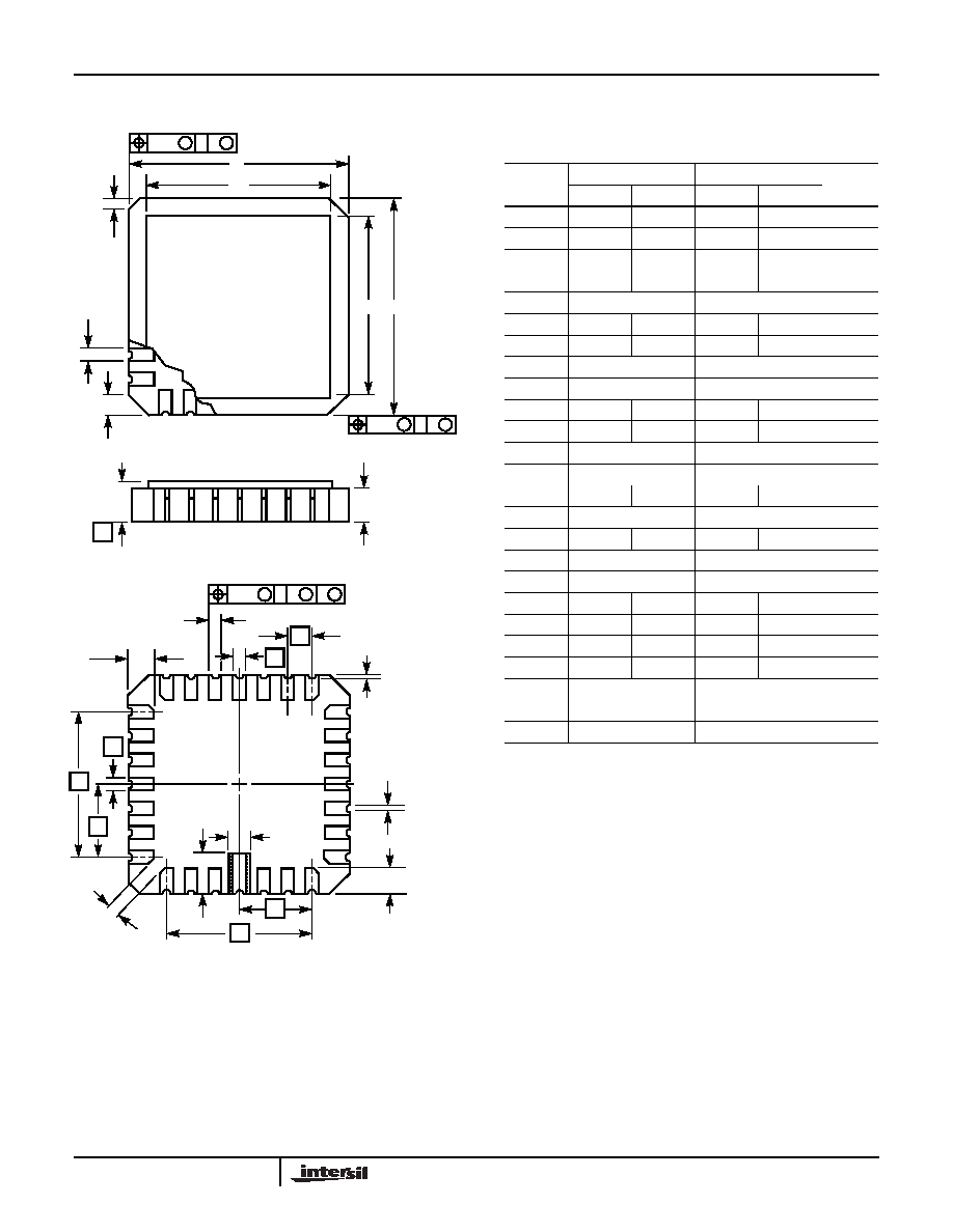
82C55A
Ceramic Leadless Chip Carrier Packages (CLCC)
D
j x 45o
D3
B
h x 45o
A
A1
E
L
L3
e
B3
L1
D2
D1
e1
E2
E1
L2
PLANE 2
PLANE 1
E3
B2
0.010
E H
S
0.010
E F
S
-E-
0.007
E F
M
S HS
B1
-H-
-F-
J44.A MIL-STD-1835 CQCC1-N44 (C-5)
44 PAD CERAMIC LEADLESS CHIP CARRIER PACKAGE
SYMBOL
INCHES
MILLIMETERS
NOTES
MIN
MAX
MIN
MAX
A
0.064
0.120
1.63
3.05
6, 7
A1
0.054
0.088
1.37
2.24
-
B
0.033
0.039
0.84
0.99
4
B1
0.022
0.028
0.56
0.71
2, 4
B2
0.072 REF
1.83 REF
-
B3
0.006
0.022
0.15
0.56
-
D
0.640
0.662
16.26
16.81
-
D1
0.500 BSC
12.70 BSC
-
D2
0.250 BSC
6.35 BSC
-
D3
-
0.662
-
16.81
2
E
0.640
0.662
16.26
16.81
-
E1
0.500 BSC
12.70 BSC
-
E2
0.250 BSC
6.35 BSC
-
E3
-
0.662
-
16.81
2
e
0.050 BSC
1.27 BSC
-
e1
0.015
-
0.38
-
2
h
0.040 REF
1.02 REF
5
j
0.020 REF
0.51 REF
5
L
0.045
0.055
1.14
1.40
-
L1
0.045
0.055
1.14
1.40
-
L2
0.075
0.095
1.90
2.41
-
L3
0.003
0.015
0.08
0.38
-
ND
11
3
NE
11
3
N44
44
3
Rev. 0 5/18/94
NOTES:
1. Metallized castellations shall be connected to plane 1 terminals
and extend toward plane 2 across at least two layers of ceramic
or completely across all of the ceramic layers to make electrical
connection with the optional plane 2 terminals.
2. Unless otherwise specified, a minimum clearance of 0.015 inch
(0.38mm) shall be maintained between all metallized features
(e.g., lid, castellations, terminals, thermal pads, etc.)
3. Symbol “N” is the maximum number of terminals. Symbols “ND”
and “NE” are the number of terminals along the sides of length
“D” and “E”, respectively.
4. The required plane 1 terminals and optional plane 2 terminals (if
used) shall be electrically connected.
5. The corner shape (square, notch, radius, etc.) may vary at the
manufacturer’s option, from that shown on the drawing.
6. Chip carriers shall be constructed of a minimum of two ceramic
layers.
7. Dimension “A” controls the overall package thickness. The maxi-
mum “A” dimension is package height before being solder dipped.
8. Dimensioning and tolerancing per ANSI Y14.5M-1982.
9. Controlling dimension: INCH.
相关PDF资料 |
PDF描述 |
|---|---|
| 3448-59 | STRAIN RELIEF 64 POS |
| IS82C55AZ96 | IC I/O EXPANDER 24B 44PLCC |
| 3448-53 | STRAIN RELIEF 16 POS |
| CP82C55AZ | IC I/O EXPANDER 24B 40DIP |
| CP82C55A-5Z | IC I/O EXPANDER 24B 40DIP |
相关代理商/技术参数 |
参数描述 |
|---|---|
| CP82C55A-5 | 功能描述:外围驱动器与原件 - PCI PERIPH PRG-I/O 5V 5MHZ COM RoHS:否 制造商:PLX Technology 工作电源电压: 最大工作温度: 安装风格:SMD/SMT 封装 / 箱体:FCBGA-1156 封装:Tray |
| CP82C55A-5S2469 | 制造商:Rochester Electronics LLC 功能描述:- Bulk |
| CP82C55A-5Z | 功能描述:外围驱动器与原件 - PCI W/ANNEAL PERIPH PRG- I/O 5V 5MHZ COM RoHS:否 制造商:PLX Technology 工作电源电压: 最大工作温度: 安装风格:SMD/SMT 封装 / 箱体:FCBGA-1156 封装:Tray |
| CP82C55AR2489 | 制造商:Rochester Electronics LLC 功能描述:- Bulk |
| CP82C55AS2065 | 制造商:Rochester Electronics LLC 功能描述:- Bulk |
发布紧急采购,3分钟左右您将得到回复。