- 您现在的位置:买卖IC网 > PDF目录1908 > CPC5601D (IXYS Integrated Circuits Division)IC DRVR PROGRAMMABLE 16-SOIC PDF资料下载
参数资料
| 型号: | CPC5601D |
| 厂商: | IXYS Integrated Circuits Division |
| 文件页数: | 3/15页 |
| 文件大小: | 0K |
| 描述: | IC DRVR PROGRAMMABLE 16-SOIC |
| 标准包装: | 50 |
| 系列: | CPC |
| 类型: | 驱动器 |
| 电源电压: | 2.5 V ~ 5.5 V |
| 安装类型: | 表面贴装 |
| 封装/外壳: | 16-SOIC(0.295",7.50mm 宽) |
| 供应商设备封装: | 16-SOIC |
| 包装: | 管件 |
INTEGRATED CIRCUITS DIVISION
CPC5601
R04
www.ixysic.com
11
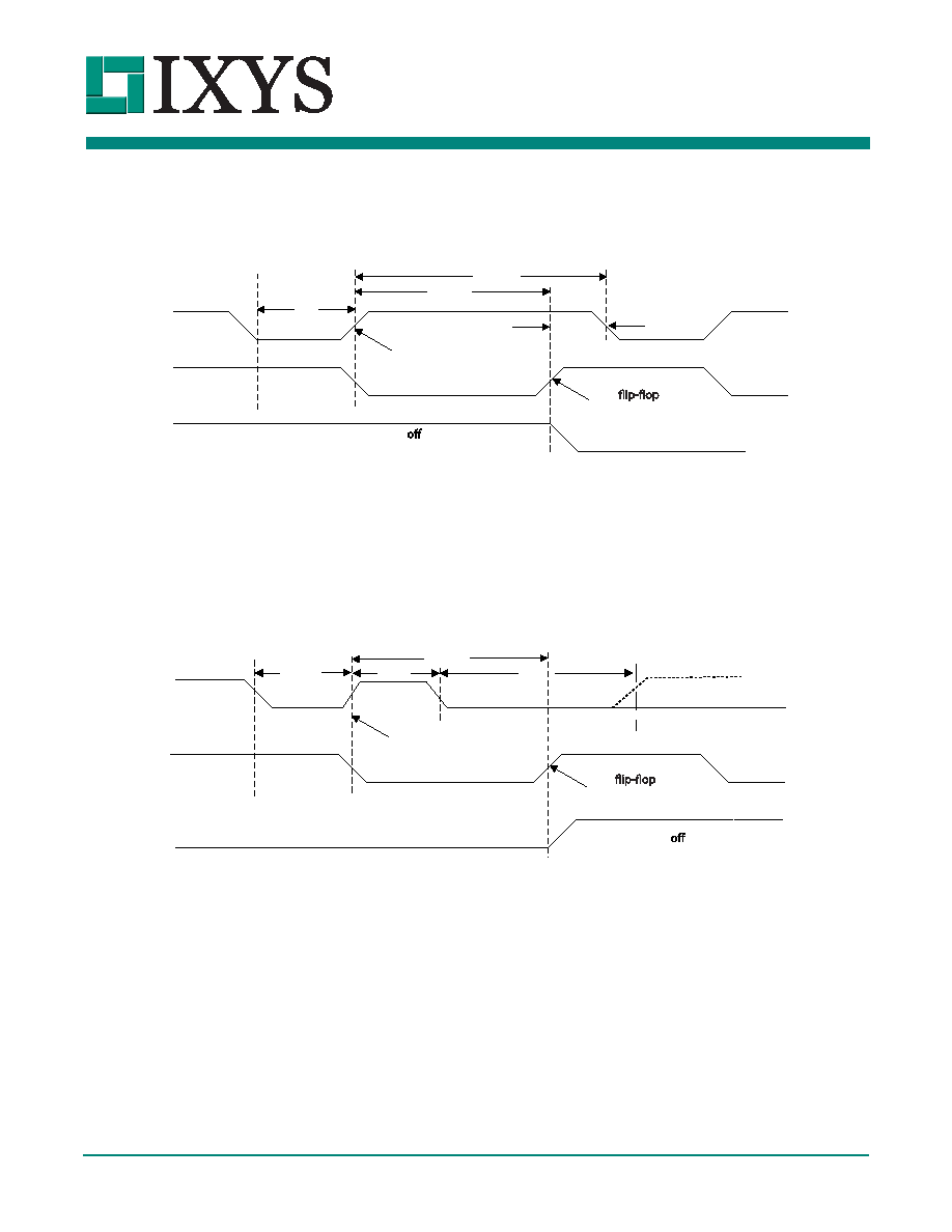
3.2 Programming Protocol
Figure 5. Latch Circuit Timing to Turn an Output On
A setup pulse on the input of at least 50
S starts the
bit programming sequence. The trailing edge of the
setup pulse starts a timer on the CPC5601 (t0). After
140
S, the value of the input is latched into the shift
register.
To set an output, hold the input high for 200
S from
the leading edge after the setup pulse. This turns on
the corresponding open-drain FET to sink current.
Figure 6. Latch Circuit Timing to Turn an Output Off
To clear an output, hold the input high for 50
S after
the setup pulse, then take the input low for at least 150
S.
Repeat the sequence of the setup pulse followed by
the appropriate input condition for each successive bit.
Bear the following in mind while programming the
CPC5601:
All bits must be set in each programming sequence,
even to change just one of the outputs.
Data is placed in least-significant bit (output 1) first.
After setting all the bits, take the input low. In the
absence of low-to-high transitions on the input, the
internal CPC5601 clock is held high, preventing any
output changes.
The CPC5601 does not employ a shift register load
function. As new data is shifted into the flip-flops, the
outputs (starting with b1) change throughout the
data input sequence.
3.3 Programming Example
This programming example sets the following
CPC5601 output state, suitable for a European DAA:
INPUT (pin 3)
CLOCK
B1 (pin 13)
140 s
200 s
B1 output FET on (sinking current)
B1 output FET (drain open)
t0
>=50 s (tsetup)
thold
Transition after setup time
initiates clock pulse
First
reads data
at the rising edge of the clock
B1 output FET (drain open)
Transition after setup time
initiates clock pulse
First
reads data
at the rising edge of the clock
INPUT (pin 3)
CLOCK
B1 (pin 13)
140 s
B1 output FET on (sinking current)
t0
50 s
>=50 s (tsetup)
150 s min
相关PDF资料 |
PDF描述 |
|---|---|
| CPC5710N | IC PHONE LINE MONITOR 8-SOIC |
| CPC5712U | PHONE LINE MON W/DETECTOR 16QSOP |
| CPC7220W | IC ANALOG SWITCH 8CH HV 28-PLCC |
| CPC7232W | IC ANALOG SWITCH 8CH HV 28-PLCC |
| CPC7514Z | IC LINE CARD ACCESS SWITC 20SOIC |
相关代理商/技术参数 |
参数描述 |
|---|---|
| CPC5601DTR | 功能描述:固态继电器-PCB安装 Programmable Driver IC, T/R RoHS:否 制造商:Omron Electronics 控制电压范围: 负载电压额定值:40 V 负载电流额定值:120 mA 触点形式:1 Form A (SPST-NO) 输出设备:MOSFET 封装 / 箱体:USOP-4 安装风格:SMD/SMT |
| CPC5602 | 制造商:CLARE 制造商全称:Clare, Inc. 功能描述:N-Channel Depletion Mode FET |
| CPC5602_12 | 制造商:CLARE 制造商全称:Clare, Inc. 功能描述:N-Channel Depletion Mode FET |
| CPC5602C | 功能描述:MOSFET MOSFET N-CHANNEL 350V RoHS:否 制造商:STMicroelectronics 晶体管极性:N-Channel 汲极/源极击穿电压:650 V 闸/源击穿电压:25 V 漏极连续电流:130 A 电阻汲极/源极 RDS(导通):0.014 Ohms 配置:Single 最大工作温度: 安装风格:Through Hole 封装 / 箱体:Max247 封装:Tube |
| CPC5602CTR | 功能描述:MOSFET N Channel Depletion Mode FET, T/R RoHS:否 制造商:STMicroelectronics 晶体管极性:N-Channel 汲极/源极击穿电压:650 V 闸/源击穿电压:25 V 漏极连续电流:130 A 电阻汲极/源极 RDS(导通):0.014 Ohms 配置:Single 最大工作温度: 安装风格:Through Hole 封装 / 箱体:Max247 封装:Tube |
发布紧急采购,3分钟左右您将得到回复。