- 您现在的位置:买卖IC网 > PDF目录26506 > CPC7592BCTR (CLARE INC) PDF资料下载
参数资料
| 型号: | CPC7592BCTR |
| 厂商: | CLARE INC |
| 元件分类: | 通信及网络 |
| 中文描述: | SPECIALTY TELECOM CIRCUIT, PDSO16 |
| 封装: | ROHS COMPLIANT, SOIC-16 |
| 文件页数: | 6/20页 |
| 文件大小: | 588K |
| 代理商: | CPC7592BCTR |
CPC7592
14
www.clare.com
R03
2.3.5 Break-Before-Make Operation - All Versions
The second break-before-make method for the
CPC7592xA/B is also the only method available for
the CPC7592xC. As shown in “CPC7592xA and
bi-directional TSD interface disables all of the
CPC7592 switches when pulled to a logic low.
Although logically disabled, an active (closed) ringing
switch (SW4) will remain closed until the next zero
crossing current event.
As shown in the table “Break-Before-Make Ringing to
page 14, this operation is similar to the one shown in
page 14, except in the method used to select the all off
state, and in when the INRINGING and INTEST inputs
are reconfigured for the talk state.
1.
Pull TSD to a logic low to end the ringing state.
This opens the ringing return switch (SW3) and
prevents any other switches from closing.
2.
Keep TSD low for at least one-half the duration of
the ringing cycle period to allow sufficient time for
a zero crossing current event to occur and for the
circuit to enter the break-before-make state.
3.
During the TSD low period, set the INRINGING and
INTEST inputs to the talk state (0, 0).
4.
Release TSD, allowing the internal pull-up to
activate the break switches.
When using TSD as an input, the two recommended
states are “0” which overrides the logic input pins and
forces an all off state and “Z” which allows normal
switch control via the logic input pins. This requires the
use of an open-collector or open-drain type buffer.
Forcing TSD to a logic high disables the thermal
shutdown circuit and is therefore not recommended as
this could lead to device damage or destruction in the
presence of excessive tip or ring potentials.
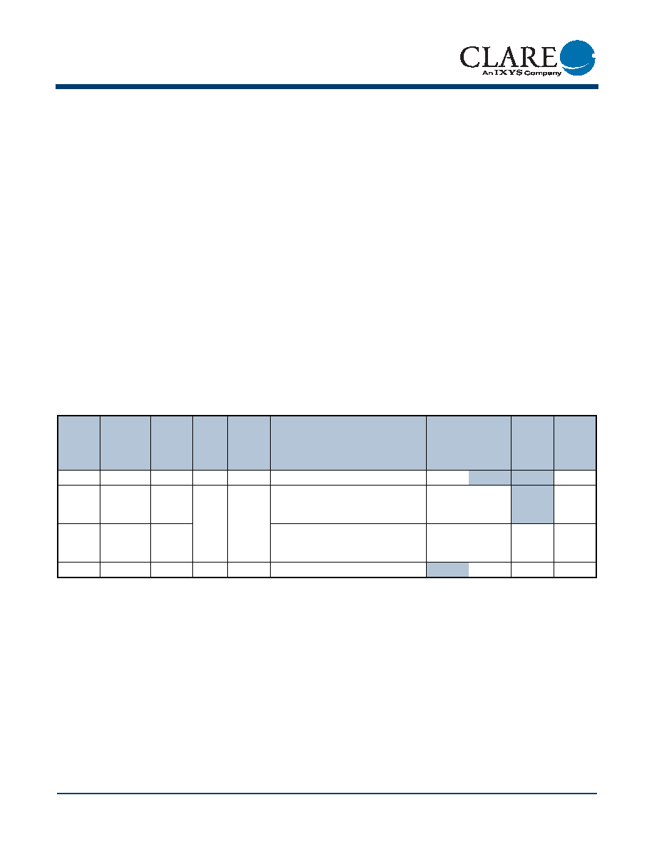
Break-Before-Make Ringing to Talk Transition Logic Sequence for all Versions
2.4 Data Latch
The CPC7592 has an integrated transparent data
latch. The latch enable operation is controlled by TTL
logic input levels at the LATCH pin. Data input to the
latch is via the input pins INRINGING and INTEST while
the output of the data latch are internal nodes used for
state control. When the LATCH enable control pin is at
a logic 0 the data latch is transparent and the input
control signals flow directly through the data latch to
the state control circuitry. A change in input will be
reflected by a change in the switch state.
Whenever the LATCH enable control pin is at logic 1,
the data latch is active and data is locked. Subsequent
changes to the input controls INRINGING and INTEST
will not result in a change to the control logic or affect
the existing switch state.
The switches will remain in the state they were in
when the LATCH changes from logic 0 to logic 1 and
will not respond to changes in input as long as the
LATCH is at logic 1. However, neither the TSD input
nor the TSD output control functions are affected by
the latch function. Since internal thermal shutdown
State
INRINGING
INTEST
LATCH
TSD
Timing
Break
Switches
Ringing
Return
Switch
(SW3)
Ringing
Switch
(SW4)
Test
Switches
Ringing
1
0
Z
-
Off
On
Off
All-Off
1
0
X0
Hold this state for at least one-half of the
ringing cycle. SW4 waiting for zero current to
turn off.
Off
On
Off
Break-
Before-
Make
0
SW4 has opened
Off
Talk
0
Z
Close Break Switches
On
Off
相关PDF资料 |
PDF描述 |
|---|---|
| CPC7592BA | |
| CPC7592BBTR | |
| CPC7593ZA | |
| CPC7593ZATR | |
| CPC7593BCTR | |
相关代理商/技术参数 |
参数描述 |
|---|---|
| CPC7592MA | 功能描述:固态继电器-PCB安装 6-pole MLP LCAS RoHS:否 制造商:Omron Electronics 控制电压范围: 负载电压额定值:40 V 负载电流额定值:120 mA 触点形式:1 Form A (SPST-NO) 输出设备:MOSFET 封装 / 箱体:USOP-4 安装风格:SMD/SMT |
| CPC7592MATR | 功能描述:固态继电器-PCB安装 6-pole MLP LCAS, T/R RoHS:否 制造商:Omron Electronics 控制电压范围: 负载电压额定值:40 V 负载电流额定值:120 mA 触点形式:1 Form A (SPST-NO) 输出设备:MOSFET 封装 / 箱体:USOP-4 安装风格:SMD/SMT |
| CPC7592MB | 功能描述:固态继电器-PCB安装 6-pole, no SCR, MLP LCAS RoHS:否 制造商:Omron Electronics 控制电压范围: 负载电压额定值:40 V 负载电流额定值:120 mA 触点形式:1 Form A (SPST-NO) 输出设备:MOSFET 封装 / 箱体:USOP-4 安装风格:SMD/SMT |
| CPC7592MBTR | 功能描述:固态继电器-PCB安装 6-pole, no SCR, MLP LCAS, T/R RoHS:否 制造商:Omron Electronics 控制电压范围: 负载电压额定值:40 V 负载电流额定值:120 mA 触点形式:1 Form A (SPST-NO) 输出设备:MOSFET 封装 / 箱体:USOP-4 安装风格:SMD/SMT |
| CPC7592MC | 功能描述:固态继电器-PCB安装 6-pole, extra logic, MLP LCAS RoHS:否 制造商:Omron Electronics 控制电压范围: 负载电压额定值:40 V 负载电流额定值:120 mA 触点形式:1 Form A (SPST-NO) 输出设备:MOSFET 封装 / 箱体:USOP-4 安装风格:SMD/SMT |
发布紧急采购,3分钟左右您将得到回复。