参数资料
| 型号: | CQ82C55A |
| 厂商: | Intersil |
| 文件页数: | 24/29页 |
| 文件大小: | 0K |
| 描述: | IC I/O EXPANDER 24B 44MQFP |
| 标准包装: | 96 |
| 接口: | 可编程 |
| 输入/输出数: | 24 |
| 中断输出: | 无 |
| 电源电压: | 4.5 V ~ 5.5 V |
| 工作温度: | 0°C ~ 70°C |
| 安装类型: | 表面贴装 |
| 封装/外壳: | 44-QFP |
| 供应商设备封装: | 44-MQFP(10x10) |
| 包装: | 管件 |
第1页第2页第3页第4页第5页第6页第7页第8页第9页第10页第11页第12页第13页第14页第15页第16页第17页第18页第19页第20页第21页第22页第23页当前第24页第25页第26页第27页第28页第29页
4
FN2969.10
November 16, 2006
Functional Description
Data Bus Buffer
This three-state bidirectional 8-bit buffer is used to interface
the 82C55A to the system data bus. Data is transmitted or
received by the buffer upon execution of input or output
instructions by the CPU. Control words and status
information are also transferred through the data bus buffer.
Read/Write and Control Logic
The function of this block is to manage all of the internal and
external transfers of both Data and Control or Status words.
It accepts inputs from the CPU Address and Control busses
and in turn, issues commands to both of the Control Groups.
(CS) Chip Select. A “low” on this input pin enables the
communication between the 82C55A and the CPU.
(RD) Read. A “low” on this input pin enables 82C55A to send
the data or status information to the CPU on the data bus. In
essence, it allows the CPU to “read from” the 82C55A.
(WR) Write. A “low” on this input pin enables the CPU to
write data or control words into the 82C55A.
(A0 and A1) Port Select 0 and Port Select 1. These input
signals, in conjunction with the RD and WR inputs, control
the selection of one of the three ports or the control word
register. They are normally connected to the least significant
bits of the address bus (A0 and A1).
(RESET) Reset. A “high” on this input initializes the control
register to 9Bh and all ports (A, B, C) are set to the input
mode. “Bus hold” devices internal to the 82C55A will hold
the I/O port inputs to a logic “1” state with a maximum hold
current of 400
μA.
Group A and Group B Controls
The functional configuration of each port is programmed by
the systems software. In essence, the CPU “outputs” a
control word to the 82C55A. The control word contains
information such as “mode”, “bit set”, “bit reset”, etc., that
initializes the functional configuration of the 82C55A.
Each of the Control blocks (Group A and Group B) accepts
“commands” from the Read/Write Control logic, receives
“control words” from the internal data bus and issues the
proper commands to its associated ports.
Control Group A - Port A and Port C upper (C7 - C4)
Control Group B - Port B and Port C lower (C3 - C0)
The control word register can be both written and read as
shown in the “Basic Operation” table. Figure 4 shows the
control word format for both Read and Write operations.
When the control word is read, bit D7 will always be a logic
“1”, as this implies control word mode information.
Ports A, B, and C
The 82C55A contains three 8-bit ports (A, B, and C). All can
be configured to a wide variety of functional characteristics
by the system software but each has its own special features
or “personality” to further enhance the power and flexibility of
the 82C55A.
Port A One 8-bit data output latch/buffer and one 8-bit data
input latch. Both “pull-up” and “pull-down” bus-hold devices
are present on Port A. See Figure 2A.
Port B One 8-bit data input/output latch/buffer and one 8-bit
data input buffer. See Figure 2B.
Port C One 8-bit data output latch/buffer and one 8-bit data
input buffer (no latch for input). This port can be divided into
82C55A BASIC OPERATION
A1
A0
RD
WR
CS
INPUT OPERATION
(READ)
00010
Port A
→ Data Bus
01010
Port B
→ Data Bus
10010
Port C
→ Data Bus
11010
Control Word
→ Data Bus
OUTPUT OPERATION
(WRITE)
00100
Data Bus
→ Port A
01100
Data Bus
→ Port B
10100
Data Bus
→ Port C
11100
Data Bus
→ Control
DISABLE FUNCTION
XXXX
1
Data Bus
→ Three-State
X
110
Data Bus
→ Three-State
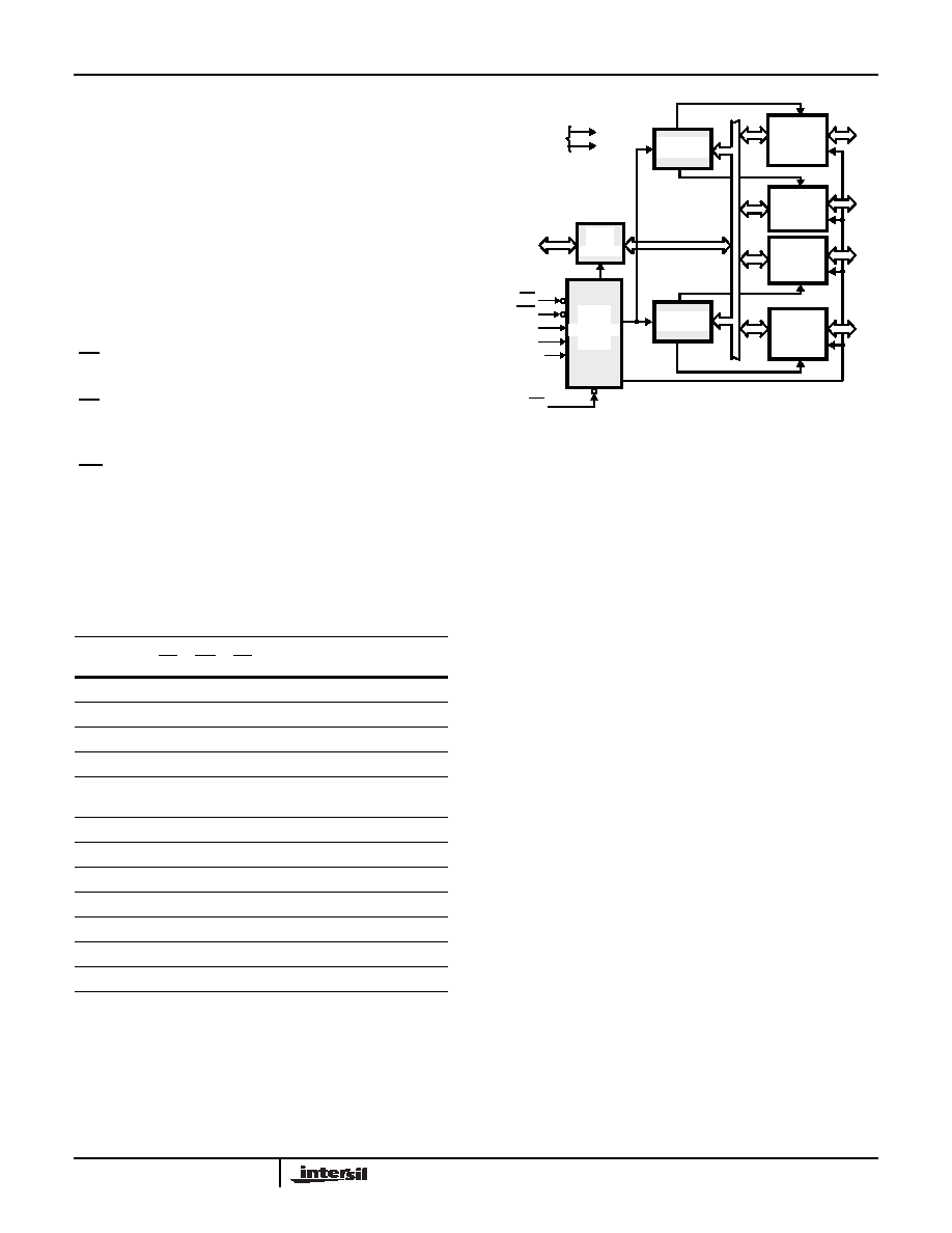
FIGURE 1. 82C55A BLOCK DIAGRAM. DATA BUS BUFFER,
READ/WRITE, GROUP A & B CONTROL LOGIC
FUNCTIONS
GROUP A
PORT A
(8)
GROUP A
PORT C
UPPER
(4)
GROUP B
PORT C
LOWER
(4)
GROUP B
PORT B
(8)
GROUP B
CONTROL
GROUP A
CONTROL
DATA
READ
WRITE
CONTROL
LOGIC
RD
WR
A1
A0
RESET
CS
D7-D0
POWER
SUPPLIES
+5V
GND
BIDIRECTIONAL
DATA BUS
I/O
PA7-
I/O
PC7-
I/O
PC3-
I/O
PB7-
BUFFER
BUS
PB0
PC0
PC4
PA0
8-BIT
INTERNAL
DATA BUS
82C55A
相关PDF资料 |
PDF描述 |
|---|---|
| ATMEGA88PV-10MUR | MCU AVR 8KB FLASH 10MHZ 32QFN |
| PCA9535EMTTXG | 16-BIT I/O EXPANDER |
| JLC1562BFEL | IC BUS INTRFACE I2C I/O 16SOEIAJ |
| ATMEGA8515-16JUR | MCU AVR 8KB FLASH 16MHZ 44PLCC |
| PCA9555D/G-T | IC I/O EXPANDER I2C 16B 24SOIC |
相关代理商/技术参数 |
参数描述 |
|---|---|
| CQ82C55A96 | 功能描述:IC I/O EXPANDER 24B 44MQFP RoHS:否 类别:集成电路 (IC) >> 接口 - I/O 扩展器 系列:- 产品培训模块:Lead (SnPb) Finish for COTS Obsolescence Mitigation Program 标准包装:74 系列:- 接口:I²C,JTAG 输入/输出数:9 中断输出:无 频率 - 时钟:400kHz 电源电压:2.7 V ~ 5.5 V 工作温度:-40°C ~ 85°C 安装类型:表面贴装 封装/外壳:20-TSSOP(0.173",4.40mm 宽) 供应商设备封装:20-TSSOP 包装:管件 包括:EEPROM |
| CQ82C55AZ | 功能描述:外围驱动器与原件 - PCI PERI PRG-I/O 5V 8MHZ COM RoHS:否 制造商:PLX Technology 工作电源电压: 最大工作温度: 安装风格:SMD/SMT 封装 / 箱体:FCBGA-1156 封装:Tray |
| CQ89-2M | 制造商:CENTRAL 制造商全称:Central Semiconductor Corp 功能描述:SURFACE MOUNT 2 AMP SILICON TRIAC 600 THRU 800 VOLTS |
| CQ89-2M_10 | 制造商:CENTRAL 制造商全称:Central Semiconductor Corp 功能描述:SURFACE MOUNT 2 AMP SILICON TRIAC 600 THRU 800 VOLTS |
| CQ89-2N | 制造商:CENTRAL 制造商全称:Central Semiconductor Corp 功能描述:SURFACE MOUNT 2 AMP SILICON TRIAC 600 THRU 800 VOLTS |
发布紧急采购,3分钟左右您将得到回复。