- 您现在的位置:买卖IC网 > PDF目录170207 > CS5124XDR8 (ON SEMICONDUCTOR) 1.5 A SWITCHING CONTROLLER, 440 kHz SWITCHING FREQ-MAX, PDSO8 PDF资料下载
参数资料
| 型号: | CS5124XDR8 |
| 厂商: | ON SEMICONDUCTOR |
| 元件分类: | 稳压器 |
| 英文描述: | 1.5 A SWITCHING CONTROLLER, 440 kHz SWITCHING FREQ-MAX, PDSO8 |
| 封装: | SOIC-8 |
| 文件页数: | 10/11页 |
| 文件大小: | 168K |
| 代理商: | CS5124XDR8 |
CS5124
http://onsemi.com
8
APPLICATION INFORMATION
UVLO and Thermal Shutdown Interaction
The UVLO pin and thermal shutdown circuit share the
same internal comparator. During high temperature
operation (TJ > 100°C) the UVLO pin will interact with the
thermal shutdown circuit. This interaction increases the
turnon threshold (and hysteresis) of the UVLO circuit. If
the UVLO pin shuts down the IC during high temperature
operation, higher hysteresis (see hysteresis specification)
might be required to enable the IC.
BIAS Pin
The bias pin can be used to control VCC as shown in the
main application diagram in Figure 1. In order to provide
adequate phase margin for the bias control loop, the pole
created by the series pass transistor and the VCC bypass
capacitor should be kept above 10 kHz. The frequency of
this pole can be calculated by Formula (1).
Pole Frequency +
Transconductance of pass Transistor
2
p
CV(CC)
(1)
The Line BIAS pin shows a significant change in the
regulated VCC voltage when sinking large currents. This will
show up as poor line regulation with a low value pullup
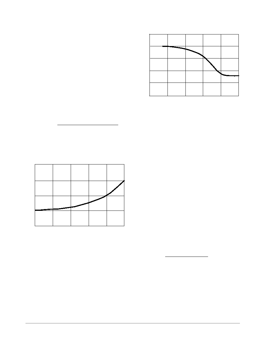
resistor. Typical regulated VCC vs BIAS pin sink current is
shown in Figure 3.
Figure 3. Regulated VCC vs. BIAS Sink Current
5.0 mΑ
10 mΑ
20 mΑ
50 mΑ
100 mΑ
200 mΑ
Bias Current (IBIAS)
V
CC
7.9
8.0
8.1
8.2
8.3
The BIAS pin and associated components form a high
impedance node. Care should be taken during PCB layout to
avoid connections that could couple noise into this node. To
ensure adequate design margin between the regulated VCC
and the Low VCC Lockout voltage, a guaranteed minimum
differential between the two values is specified (see
electrical characteristcs).
Gate Drive
Rail to rail gate driver operation can be obtained (up to
13.5 V) over a range of MOSFET input capacitance if the
gate resistor value is kept low. Figure 5 shows the high gate
drive level vs. the series gate resistance with VCC = 8.0 V
driving an IRF220.
Figure 4. Gate Drive vs. Gate Resistor Driving an
IRF220 (VCC = 8.0 V)
0
Gate Resistor Value
Peak
V
oltage
8.5
0.3
0.5
2.5
5.0
8.0
7.5
7.0
6.5
6.0
11
A large negative dv/dt on the power MOSFET drain will
couple current into the gate driver through the gate to drain
capacitance. If this current is kept within absolute maximum
ratings for the GATE pin it will not damage the IC. However
if a high negative dv/dt coincides with the start of a PWM
duty cycle, there will be small variations in oscillator
frequency due to current in the controller substrate. If
required, this can be avoided by choosing the transformer
ratio and reset circuit so that a high dv/dt does not coincide
with the start of a PWM cycle, or by clamping the negative
voltage on the GATE pin with a Schottky diode
First Current Sense Threshold
During normal operation the peak primary current is
controlled by the level of the VFB pin (as determined by the
control loop) and the current sense network. Once the signal
on the ISENSE pin exceeds the level determined by VFB pin
the PWM cycle terminates. During high output currents the
VFB pin will rise until it reaches the VFB clamp. The first
current sense threshold determines the maximum signal
allowed on the ISENSE pin before the PWM cycle is
terminated. Under this condition the maximum peak current
is determined by the VFB Clamp, the slope compensation
ramp, the PWM comparator offset voltage and the PWM on
time. The nominal first current threshold varies with on time
and can be calculated from Formulas (2) and (3) below.
1st Threshold +
2.9 V * 170 mV ms
TON
10
* 60 mV
(2)
When the output current is high enough for the ISENSE pin
to exceed the first threshold, the PWM cycle terminates
early and the converter begins to function more like a current
source. The current sense network must be chosen so that the
peak current during normal operation does not exceed the
first current sense threshold.
Second Current Sense Threshold
The second threshold is intended to protect the converter
from overheating by switching to a low duty cycle mode
when there are abnormally high fast rise currents in the
相关PDF资料 |
PDF描述 |
|---|---|
| CS5322GDWR28 | 1.5 A SWITCHING CONTROLLER, 1000 kHz SWITCHING FREQ-MAX, PDSO28 |
| CS5361GD16 | 2 A BATTERY CHARGE CONTROLLER, 635 kHz SWITCHING FREQ-MAX, PDSO16 |
| CS8413 | 96 KHZ DIGITAL AUDIO RECEIVER |
| CS8413-CS | 96 KHZ DIGITAL AUDIO RECEIVER |
| CS8414 | 96 KHZ DIGITAL AUDIO RECEIVER |
相关代理商/技术参数 |
参数描述 |
|---|---|
| CS5124XDR8G | 功能描述:电流型 PWM 控制器 Hi Performance Current Mode PWM RoHS:否 制造商:Texas Instruments 开关频率:27 KHz 上升时间: 下降时间: 工作电源电压:6 V to 15 V 工作电源电流:1.5 mA 输出端数量:1 最大工作温度:+ 105 C 安装风格:SMD/SMT 封装 / 箱体:TSSOP-14 |
| CS5126-KL | 制造商:Rochester Electronics LLC 功能描述: 制造商:Cirrus Logic 功能描述: |
| CS5126-KLZ | 制造商:Rochester Electronics LLC 功能描述: 制造商:Cirrus Logic 功能描述: |
| CS5126-KP | 制造商:Rochester Electronics LLC 功能描述:2-CH 16-BIT SUCCESSIVE APPROXIMATION ADC, - Bulk |
| CS5126XDR8 | 功能描述:IC REG CTRLR FLYBK ISO PWM 8SOIC RoHS:否 类别:集成电路 (IC) >> PMIC - 稳压器 - DC DC 切换控制器 系列:- 标准包装:4,000 系列:- PWM 型:电压模式 输出数:1 频率 - 最大:1.5MHz 占空比:66.7% 电源电压:4.75 V ~ 5.25 V 降压:是 升压:无 回扫:无 反相:无 倍增器:无 除法器:无 Cuk:无 隔离:无 工作温度:-40°C ~ 85°C 封装/外壳:40-VFQFN 裸露焊盘 包装:带卷 (TR) |
发布紧急采购,3分钟左右您将得到回复。