- 您现在的位置:买卖IC网 > PDF目录13676 > CS51412GD8G (ON Semiconductor)IC REG BUCK 1.5A 8SOIC PDF资料下载
参数资料
| 型号: | CS51412GD8G |
| 厂商: | ON Semiconductor |
| 文件页数: | 2/20页 |
| 文件大小: | 0K |
| 描述: | IC REG BUCK 1.5A 8SOIC |
| 标准包装: | 98 |
| 类型: | 降压(降压) |
| 输出数: | 1 |
| 输入电压: | 4.5 V ~ 40 V |
| PWM 型: | 混合物 |
| 频率 - 开关: | 260kHz |
| 电流 - 输出: | 1.5A |
| 同步整流器: | 无 |
| 工作温度: | 0°C ~ 70°C |
| 安装类型: | 表面贴装 |
| 封装/外壳: | 8-SOIC(0.154",3.90mm 宽) |
| 包装: | 管件 |
| 供应商设备封装: | 8-SOICN |
�� �
�
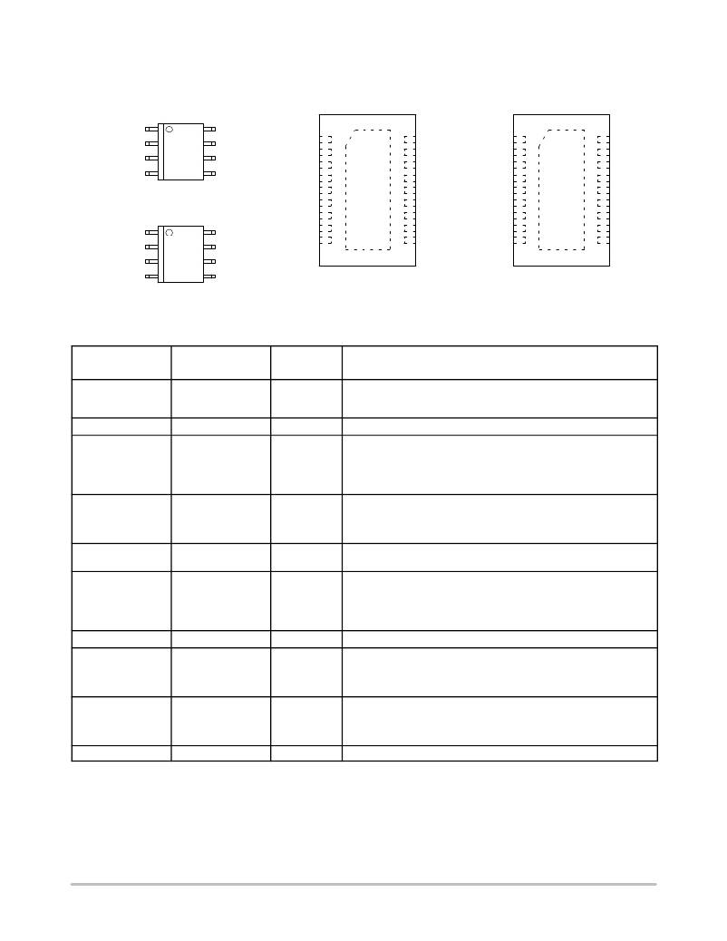
�CS51411,� CS51412,� CS51413,� CS51414�
�PIN� CONNECTIONS�
�CS51411/3�
�CS51411/3�
�CS51412/4�
�BOOST�
�V� IN�
�V� SW�
�SHDNB�
�BOOST�
�V� IN�
�1�
�1�
�8�
�CS51412/4�
�8�
�V� C�
�V� FB�
�GND�
�SYNC�
�V� C�
�V� FB�
�BOOST�
�V� IN�
�V� IN�
�V� IN�
�Vsw�
�V� SW�
�V� SW�
�SHDNB�
�NC�
�1�
�2�
�3�
�4�
�5�
�6�
�7�
�8�
�9�
�18�
�17�
�16�
�15�
�14�
�13�
�12�
�11�
�10�
�NC�
�V� C�
�V� FB�
�NC�
�NC�
�GND�
�NC�
�NC�
�SYNC�
�BOOST�
�V� IN�
�V� IN�
�V� IN�
�Vsw�
�V� SW�
�V� SW�
�BIAS�
�NC�
�1�
�2�
�3�
�4�
�5�
�6�
�7�
�8�
�9�
�18�
�17�
�16�
�15�
�14�
�13�
�12�
�11�
�10�
�NC�
�V� C�
�V� FB�
�NC�
�NC�
�GND�
�NC�
�NC�
�SHDNB�
�V� SW�
�BIAS�
�GND�
�SHDNB�
�PACKAGE� PIN� DESCRIPTION�
�SOIC� ?� 8�
�DFN18�
�Package� Pin� #�
�1�
�2�
�3�
�4�
�(CS51412/CS51414)�
�5�
�(CS51411/CS51413)�
�5�
�(CS51412/CS51414)�
�4�
�(CS51411/CS51413)�
�6�
�7�
�8�
�?�
�Package� Pin� #�
�1�
�2,� 3,� 4�
�5,� 6,� 7�
�8�
�10�
�10�
�(CS51412/CS51414)�
�8�
�(CS51411/CS51413)�
�13�
�16�
�17�
�9,� 11,� 12,� 14,� 15,� 18�
�Pin� Symbol�
�BOOST�
�V� IN�
�V� SW�
�BIAS�
�SYNC�
�SHDNB�
�GND�
�V� FB�
�V� C�
�NC�
�Function�
�The� BOOST� pin� provides� additional� drive� voltage� to� the� on� ?� chip� NPN�
�power� transistor.� The� resulting� decrease� in� switch� on� voltage� increases�
�efficiency.�
�This� pin� is� the� main� power� input� to� the� IC.�
�This� is� the� connection� to� the� emitter� of� the� on� ?� chip� NPN� power� transistor�
�and� serves� as� the� switch� output� to� the� inductor.� This� pin� may� be�
�subjected� to� negative� voltages� during� switch� off� ?� time.� A� catch� diode� is�
�required� to� clamp� the� pin� voltage� in� normal� operation.� This� node� can�
�stand� ?� 1.0� V� for� less� than� 50� ns� during� switch� node� flyback.�
�The� BIAS� pin� connects� to� the� on� ?� chip� power� rail� and� allows� the� IC� to� run�
�most� of� its� internal� circuitry� from� the� regulated� output� or� another� low�
�voltage� supply� to� improve� efficiency.� The� BIAS� pin� is� left� floating� if� this�
�feature� is� not� used.�
�This� pin� provides� the� synchronization� input.�
�Shutdown_bar� input.� This� is� an� active� ?� low� logical� input,� TTL� compatible,�
�with� an� internal� pull� ?� up� current� source.� The� IC� goes� into� sleep� mode,�
�drawing� less� than� 85� m� A� when� the� pin� voltage� is� pulled� below� 1.0� V.� This�
�pin� may� be� left� floating� in� applications� where� a� shutdown� function� is� not�
�required.�
�Power� return� connection� for� the� IC.�
�The� FB� pin� provides� input� to� the� inverting� input� of� the� error� amplifier.� If�
�V� FB� is� lower� than� 0.29� V,� the� oscillator� frequency� is� divided� by� four,� and�
�current� limit� folds� back� to� about� 1� A.� These� features� protect� the� IC� under�
�severe� overcurrent� or� short� circuit� conditions.�
�The� V� C� pin� provides� a� connection� point� to� the� output� of� the� error�
�amplifier� and� input� to� the� PWM� comparator.� Driving� of� this� pin� should� be�
�avoided� because� on� ?� chip� test� circuitry� becomes� active� whenever�
�current� exceeding� 0.5� mA� is� forced� into� the� IC.�
�No� Connection�
�http://onsemi.com�
�2�
�相关PDF资料 |
PDF描述 |
|---|---|
| EMC12DREN-S734 | CONN EDGECARD 24POS .100 EYELET |
| EMC12DREH-S734 | CONN EDGECARD 24POS .100 EYELET |
| CS51411GD8G | IC REG BUCK 1.5A 8SOIC |
| MAX6728AKASDD3+T | IC SUPERVISOR MPU SOT23-8 |
| ECC15DRAS-S734 | CONN EDGECARD 30POS .100 R/A PCB |
相关代理商/技术参数 |
参数描述 |
|---|---|
| CS51412GDR8 | 功能描述:直流/直流开关调节器 1.5A Low Voltage RoHS:否 制造商:International Rectifier 最大输入电压:21 V 开关频率:1.5 MHz 输出电压:0.5 V to 0.86 V 输出电流:4 A 输出端数量: 最大工作温度: 安装风格:SMD/SMT 封装 / 箱体:PQFN 4 x 5 |
| CS51412GDR8G | 功能描述:直流/直流开关调节器 1.5A Low Voltage Buck RoHS:否 制造商:International Rectifier 最大输入电压:21 V 开关频率:1.5 MHz 输出电压:0.5 V to 0.86 V 输出电流:4 A 输出端数量: 最大工作温度: 安装风格:SMD/SMT 封装 / 箱体:PQFN 4 x 5 |
| CS51412GMNR2G | 功能描述:直流/直流开关调节器 1.5A 260kHz BUCK REG LOW VOLTAGE RoHS:否 制造商:International Rectifier 最大输入电压:21 V 开关频率:1.5 MHz 输出电压:0.5 V to 0.86 V 输出电流:4 A 输出端数量: 最大工作温度: 安装风格:SMD/SMT 封装 / 箱体:PQFN 4 x 5 |
| CS51413ED8 | 功能描述:直流/直流开关调节器 1.5A Low Voltage RoHS:否 制造商:International Rectifier 最大输入电压:21 V 开关频率:1.5 MHz 输出电压:0.5 V to 0.86 V 输出电流:4 A 输出端数量: 最大工作温度: 安装风格:SMD/SMT 封装 / 箱体:PQFN 4 x 5 |
| CS51413ED8G | 功能描述:直流/直流开关调节器 1.5A Low Voltage Buck RoHS:否 制造商:International Rectifier 最大输入电压:21 V 开关频率:1.5 MHz 输出电压:0.5 V to 0.86 V 输出电流:4 A 输出端数量: 最大工作温度: 安装风格:SMD/SMT 封装 / 箱体:PQFN 4 x 5 |
发布紧急采购,3分钟左右您将得到回复。